Input Devices
Table of content:
1 - Final project board | attiny16141.1 - selecting IC 1.2 - designing 1.3 - generating toolpath 1.4 - milling
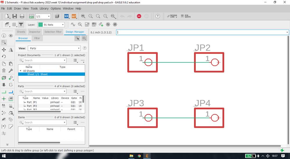
2 - updi-d11c
2.1 - designing 2.2 - milling 2.3 - soldering attiny1614 and updi-samd11c board
3 - Programming
4 - updi-ft230xs
5 - application
5.1 - Serial monitor 5.2 - ultrasonic sensor 5.3 - Rain drop sensor 5.4 - step response
6 - Group assignment
In this week of input devices we were suppose to add a sensor to the microcontroller board that i have designed and read the outcome. In the
output device week i had designed a circuit board specially for the output devices i had explored that week. For this week, instead of
exploring different components and designing the circuit board specially for operating input devices and then desgin another board for the final
project, i decided to designed the circuit board for my final project in this week.
I had a discussion with my local instructor regarding the sensore/components that are going to be used for my final project. My final project
circuit board will be divided in main two parts,
imput part
FOr the input part, i need to detect motion/movement and water. For the movement/motion, i tested the ultrasonic sensor and PIR sensor with my
UNO and either i was ddoing it wrong or that's how PIR sensor works but I was finding it very difficult working with PIR sensor. It sometimes
detect
even the slightest of the movement instantly and sometimes it just won't give any feedback. SOmetimes after detecting the movementor, it will
give some feedback
very late and so i was more comfortable with selecting ultrasonic sensor as it was easy to operate and i was able to get the reading in the form
of distance.
For detecting the water, i decided to give the provision for both, the raindrop sensor and the step response. For some reasons, i had to first
make the final project board without spending too much time exploring the input devices and that is the reason i didn't tested the raindrop sensor
and the step response and finalize which sensor i am going to use for my final project on the basis of the results i got and hence gave the provision
for both.
output part
For the output part, i had to give the feedback after detecting the leakage. For the instant feedback i decided to use LED and Buzzer. And to read
the data regarding the leakage, i decided to use OLED. I was even planning to send the data throughan app and so i considered to give proviison
for the wifi modeule while designing the board.
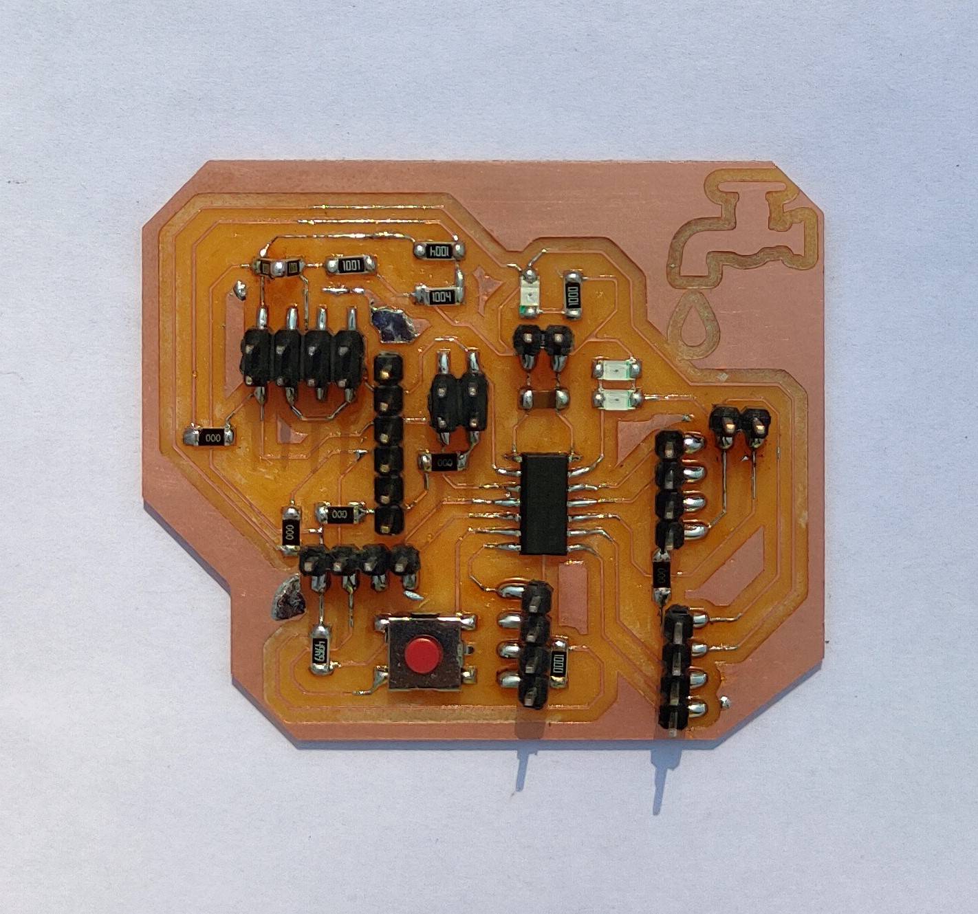
final project board | attiny1614
Selecting IC
With all the components decided, i had to decide what IC i will use for my final project circuit board. I wanted to use OLED so i had to look
for the IC with I2C protocol/ has SDA & SCl pins. I wanted to use a wifi module and step response so i had to look for TX and RX pins in the IC.
So apart from wifi module/step response and OLED i was going to require 2 prpgrammable pins for led and buzzer, 2 programmable pins for
ultrasonic sensor, 2 programmable pins for rain drop sensor(one of which should be analog) so 12-14 pins would be sufficient for my project.
In the output devices i had designed a board with attiny44 ic and i wasn't able to upload the sketch of the OLED and i was not able to display
anything onto the LCD. So after exploring a bit i decided to use the attiny1614 ic because it had all the things that were required for my
project.
attiny1614 has
14 pins. 10 of which are analog/digital and 6 of them are PWM pins.
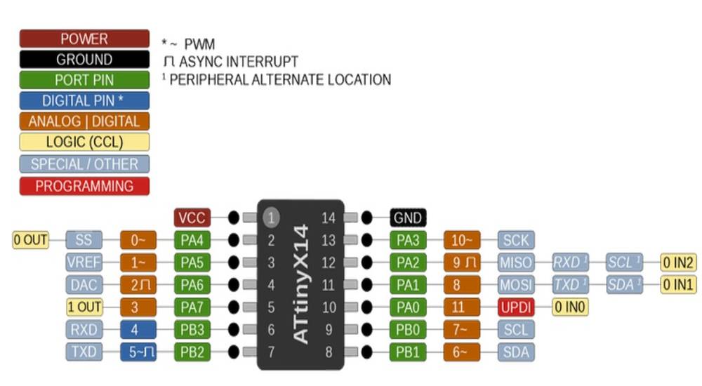
2Kb of SRAM.
16 Kb of FLASH.
256 Bytes of EEPROM
and here are the provision for SDA/SCL and TX/RX pins,
designing
I designed the schematic and board in eagle. As decided i gave all the provisions for the header pins(for mounting module) and componnets and
this was the schematic i ended up with,
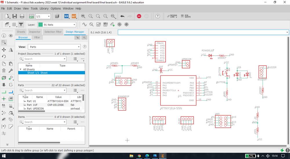
I then confirmed with my local instructor if everything is correct with the schematic and when he approved, i started routing the board.
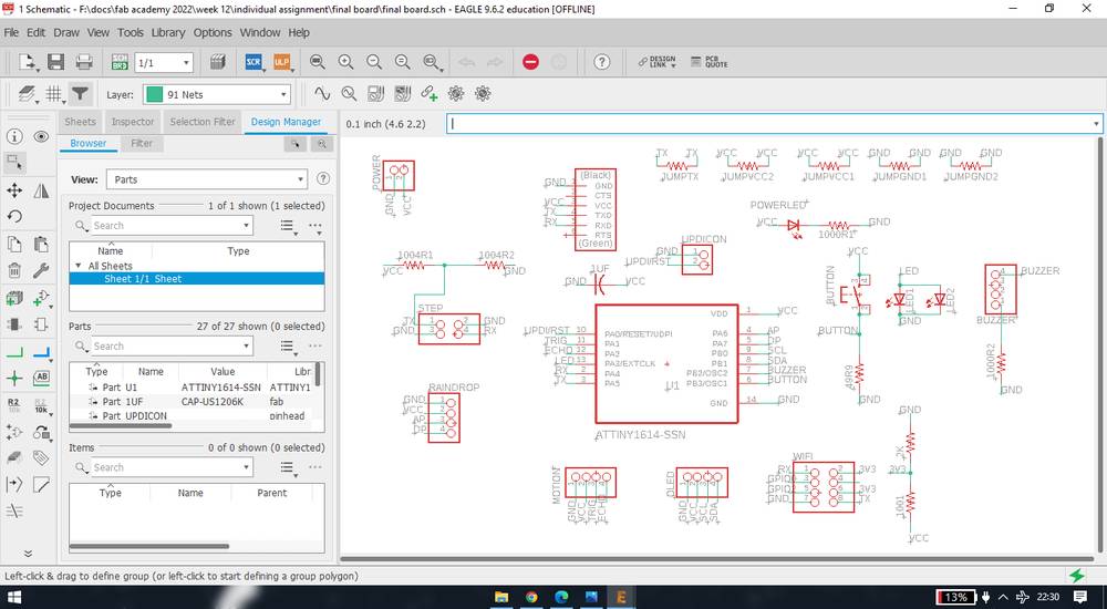
After routing for few hours, i had to add 5 jumpers in order to give all the connections. This was my connection after adding 5
jumpers,
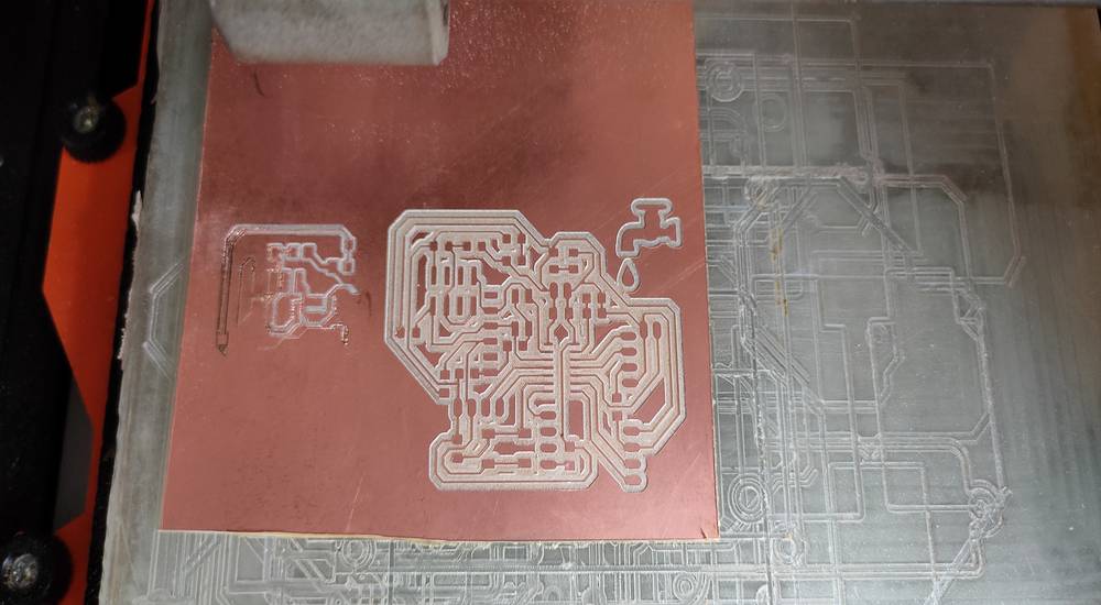
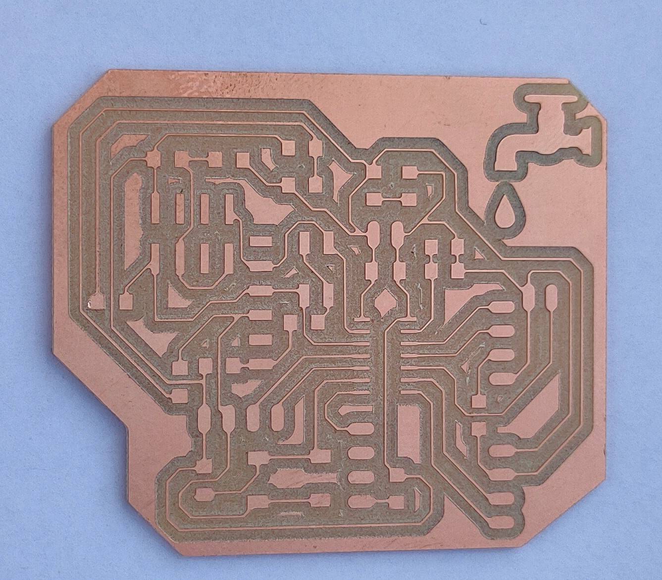
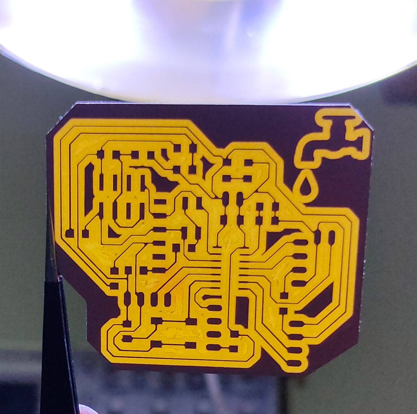
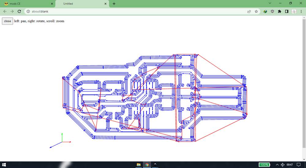
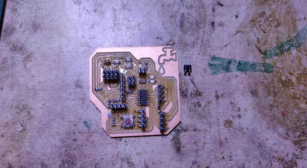
This is how my board looks like,
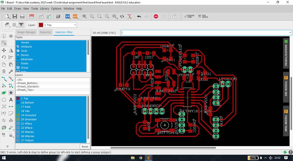
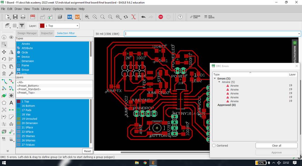
I was getting airwire error at the places where i had placed the resistor as jumper. I was getting the same error at the time of making hello
world board so i didn't spend much time removing the error.
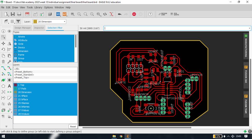
I then gave the border for the outline of PCB,
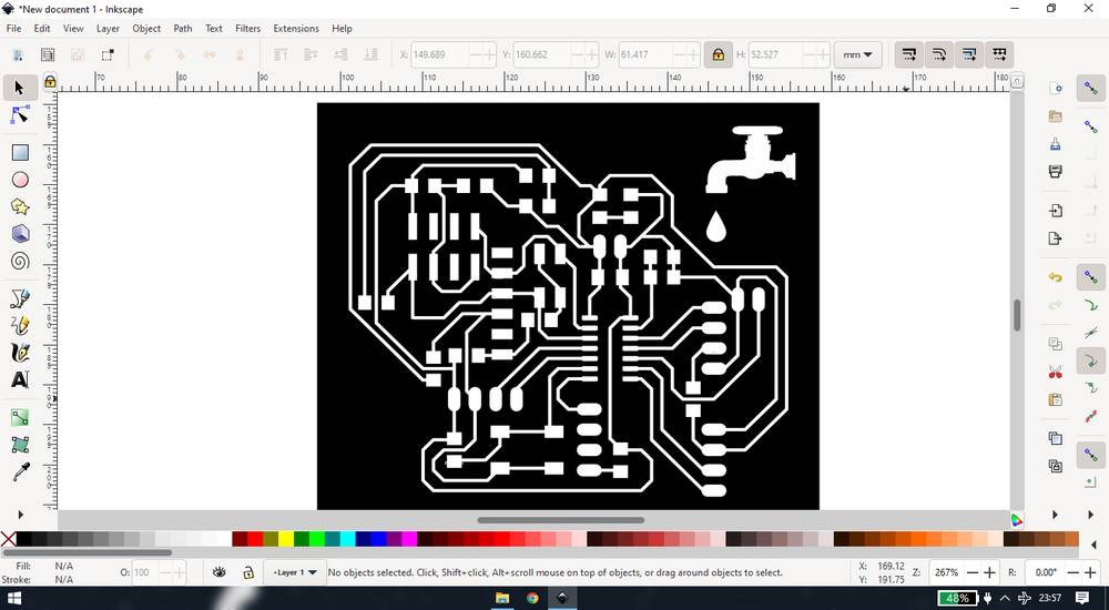
I then wanted add some logo regarding my final project so i first exported the inner and outer image(png) of the board and added a logo in inkscape.
I downloaded the image from https://pixabay.com/ . Since the traces are white when exported as monochrome from the eagle, i needed to convert
the image to monochrome too(white) so i converted the image into monochrome from this website: https://manytools.org/image/colorize-filter/ .
I then inserted the logo into my PCB in inkscape.
library installed:
pinheader: https://github.com/zumbik/Eagle-Libraries/blob/master/pinhead-2.lbr
attiny1614: https://www.snapeda.com/parts/ATTINY1614-SSNR/Atmel/view-part/
generating toolpath
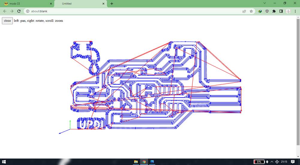
I used mods community project: http://modsproject.org/ for generating the toolpath/rml file and vpanel software for communicating with the
machine.
Visit the mods community project website and go to programs > open programs > PCB CBA(under SRM-20 mill) and Upload png file of the inner
trace under "read png". Don't forget to check the dpi of the image, it should be 1000dpi.
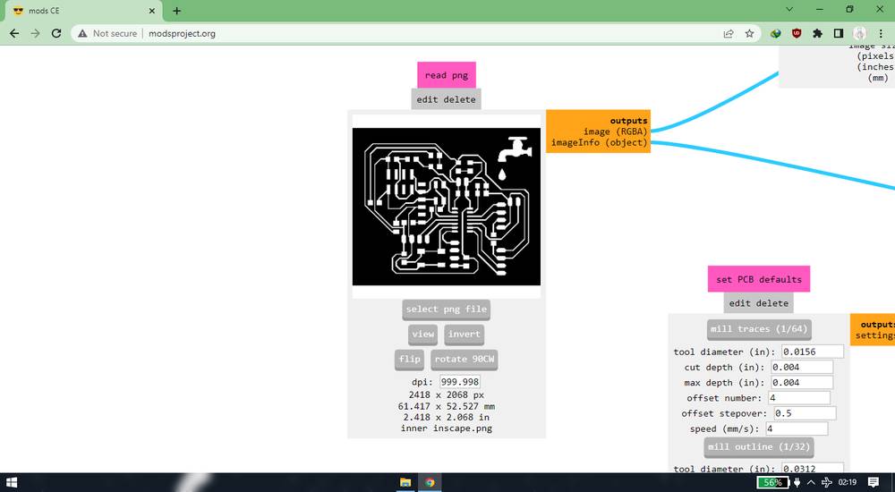
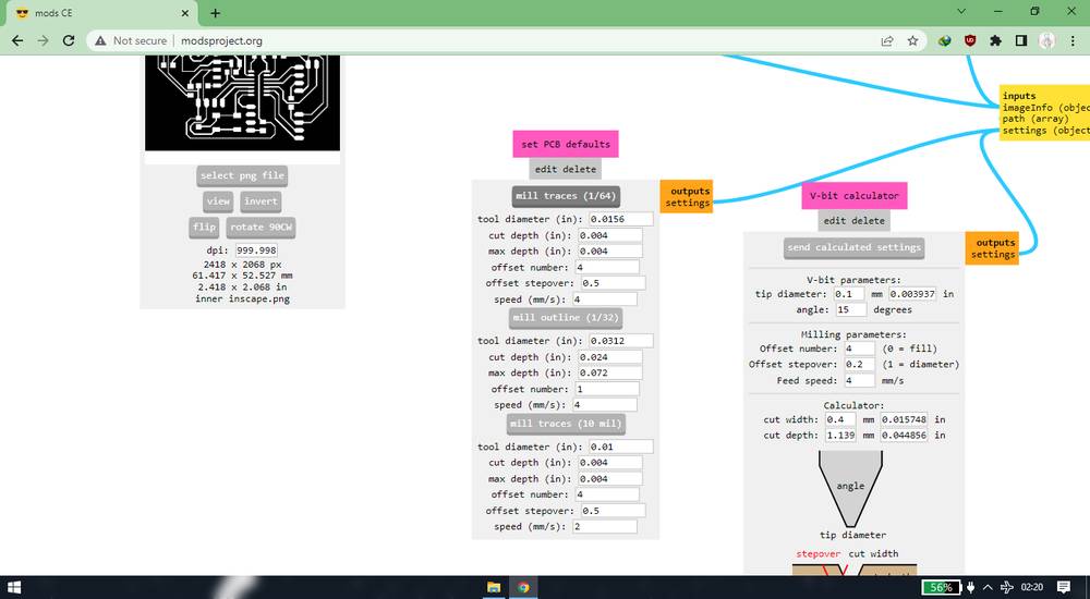
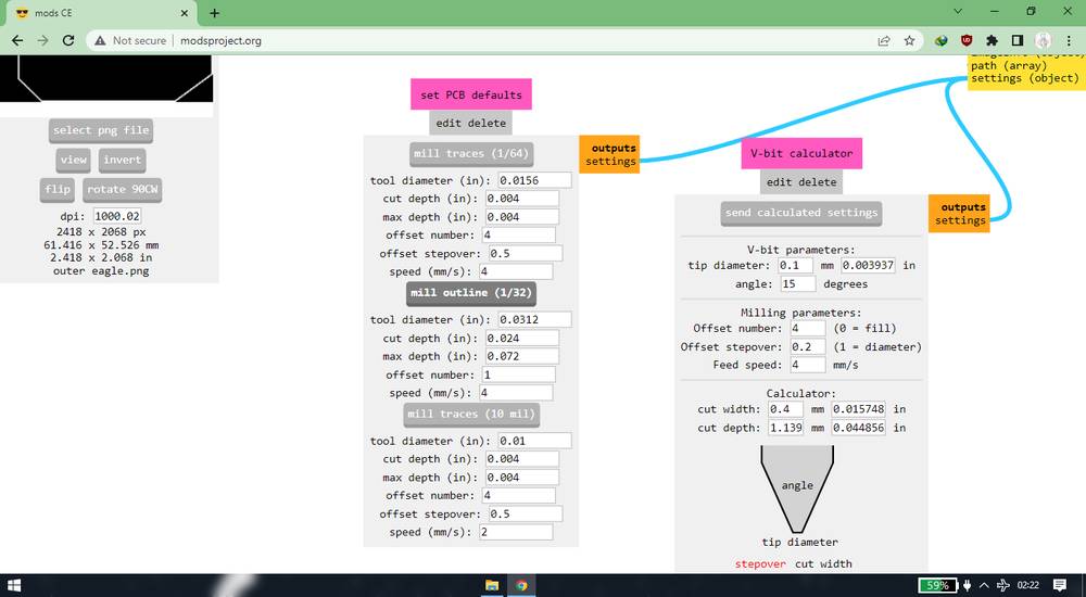
select mill traces 1/64 under "set PCB defaults"
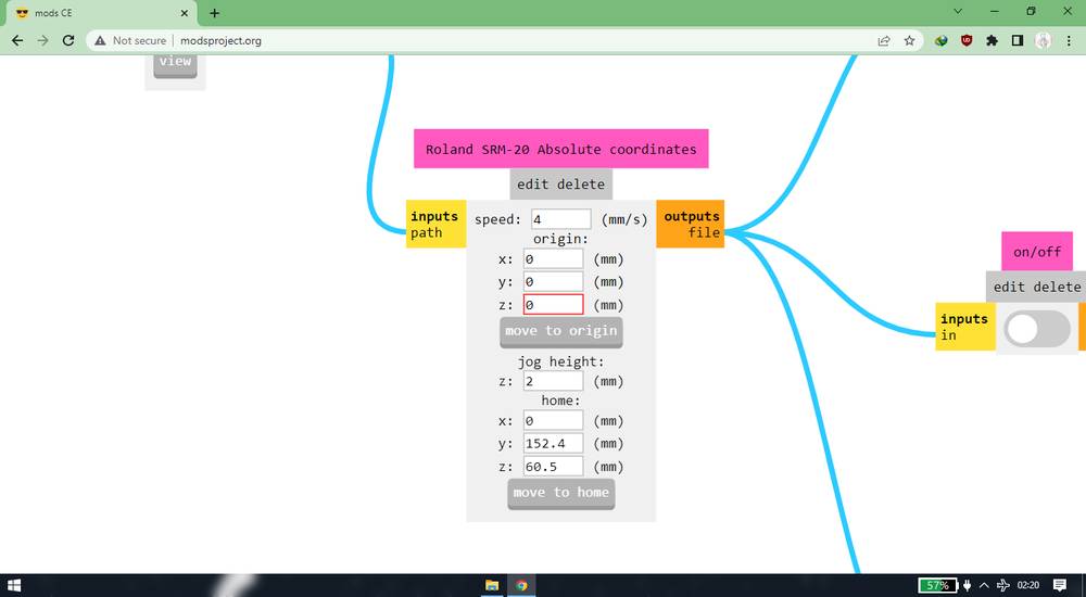
set the "Roland SRM-20 Absolute coordinates" to 0 for X, Y and Z axis,
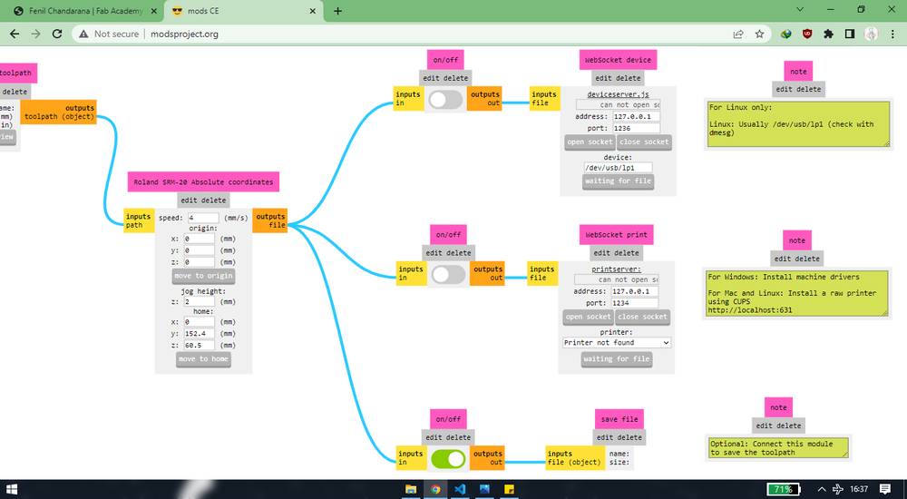
Disable both, the websocket device and websocket print and enable the save file option,
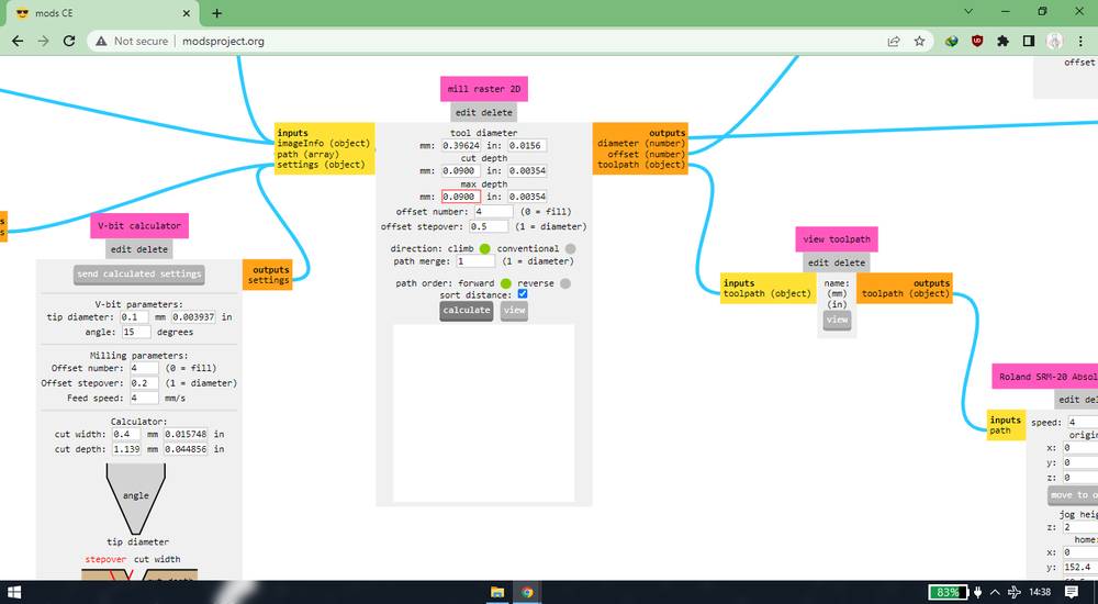
I set the cut depth and max depth as 0.0800mm while using VBIT and set the offset number to 4,
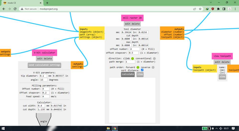
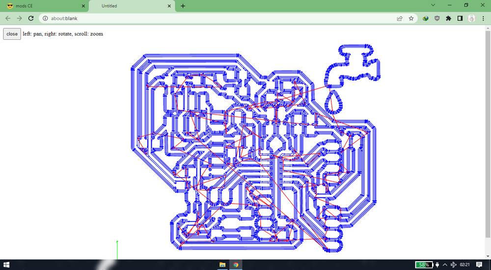
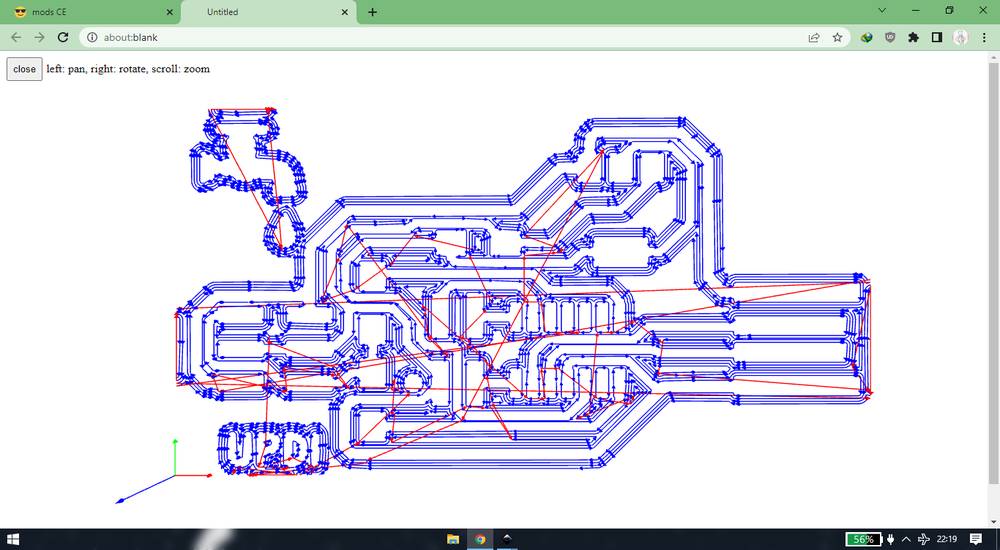
this was the preview after i hit calculate,
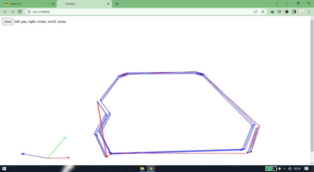
For generating toolpath for outer trace, i selected mill outline 1/32 under "set PCB defaults and apart from that i kept the rest of the settings
as it is,
this was the preview of the outline trace,
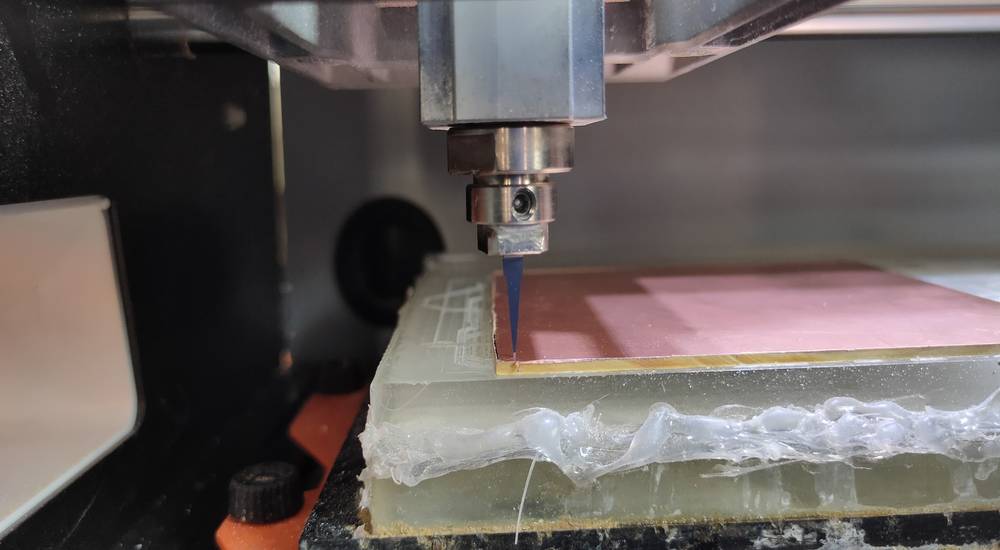
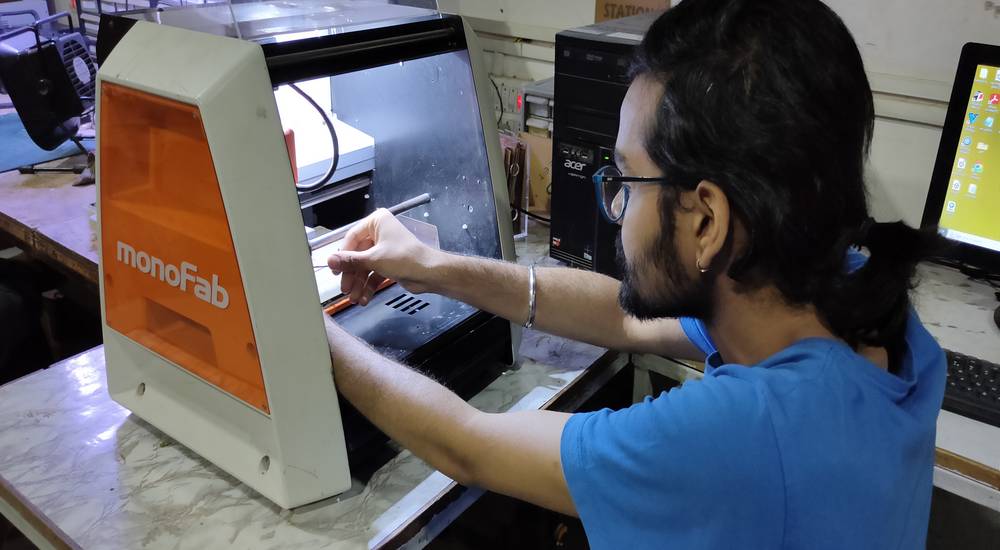
milling
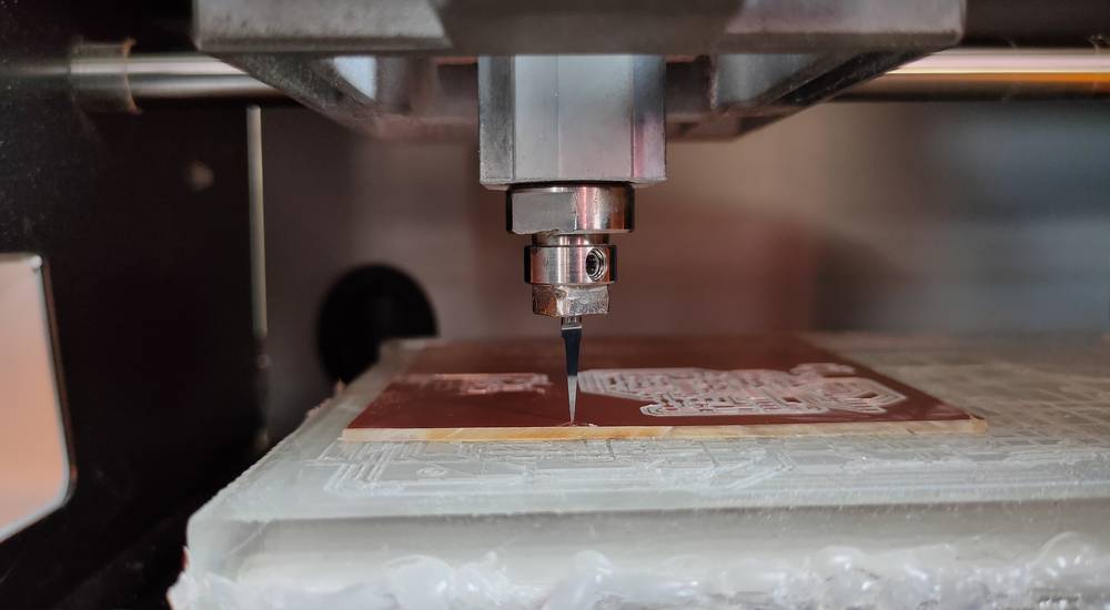
For milling the PCB i used the broken VBIT from the previous assignment. I don't know how much i have explained about these broken VBIT but i'll
explain once again in brief: So the VBIT we were using till now was the 30° VBIT which is very pointy and from using numerous VBIT's i can say that
the tip of the VBIT is bound to be broken if you generate the toolpath with the default settings of 0.1016mm cut depth and max depth. If a large
chunk of the vbit gets broken, you won't be able to use it afterwards and if youdo use it, you'll get the PCB full of burr. So the goal is
to try to break a very small amount of vbit. In order to achieve that, what we use to do was reduce the cut depth and max depth to 0.0800mm. If
we were using a fresh vbit it would break once(or twice if we are unlucky). After the VBIT breaks set the Z axis coordinate again and re-trace
and then you will get fine results with the broken VBIT.
This is the position of the VBIT inside the collet,
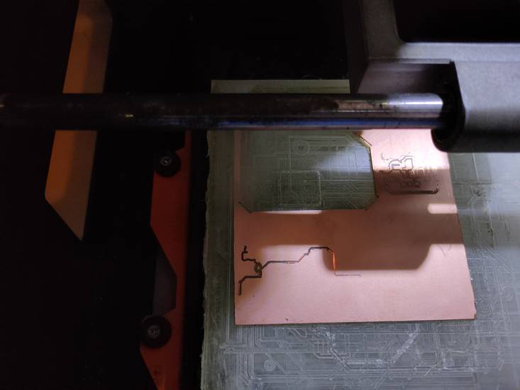
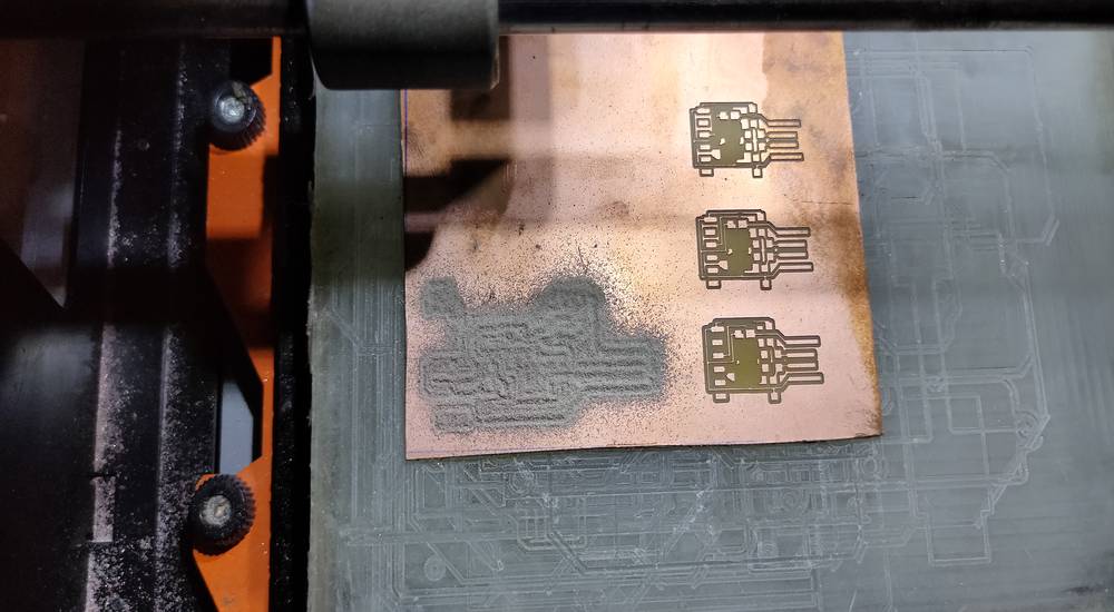
This time, unlike previous traces, the vbit was not able to remove the copper layer with 0.0800mm cut depth,
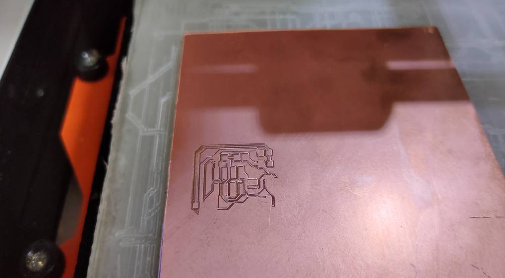
I was able to see the trace but the surface of the copper clad was smooth without any grooves. I retrace the inner file again and was getting
the same results. I then generated the toolpath again with 0.0900mm cut depth and max depth, (however the vpanel was showing -0.10 as z axis
coordinates while tracing)
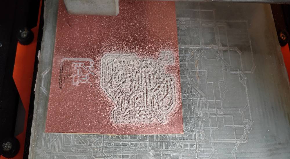
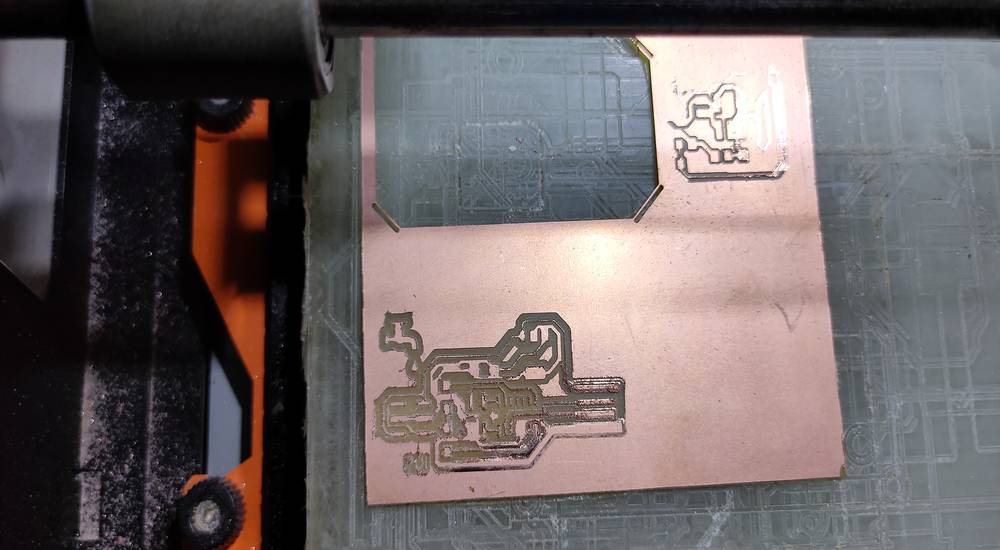
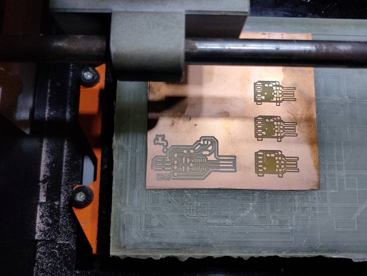
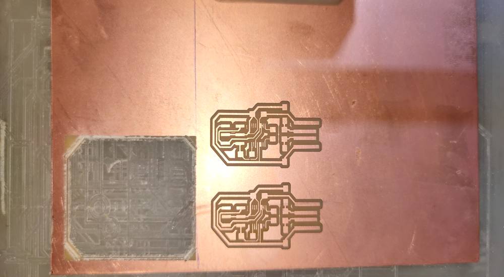
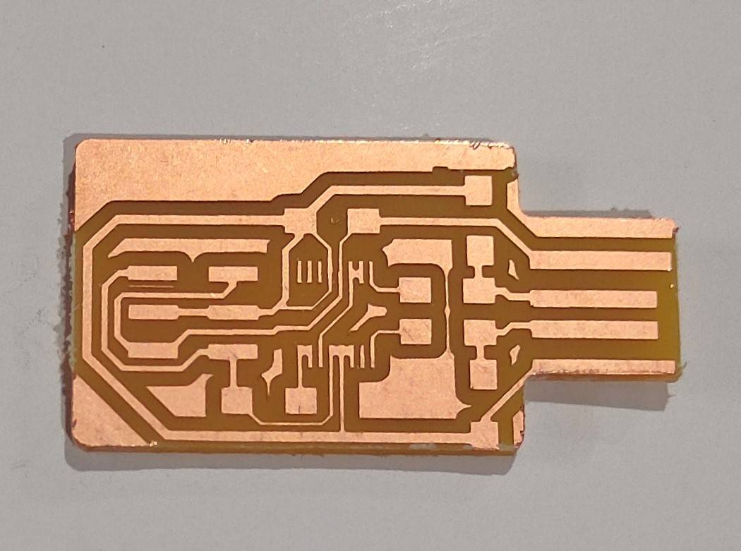
with the new toolpath of 0.0900mm cut depth and max depth, i started tracing again and this is the result,
and this was the position of the vbit inside the collet,
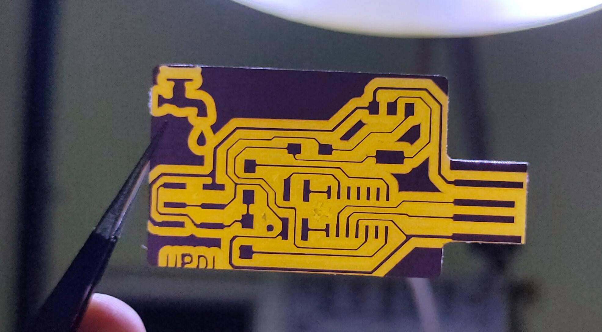
this is the result after tracing the outline of the PCB,
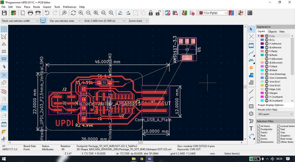
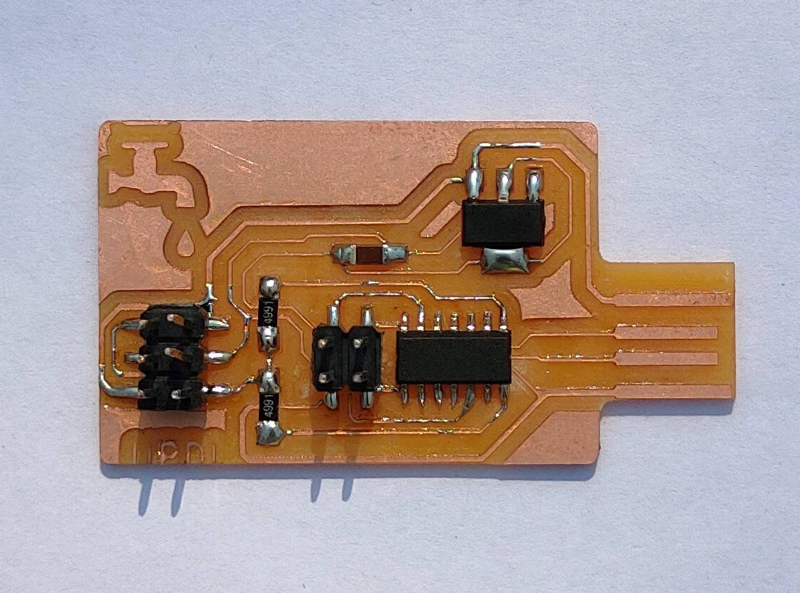
updi d11c
My instructor told me that in order to program the final project board(attiny1614) i would require a programmer - UPDI(SAMD11C14) and it
was decided for me to re-design and mill this particular UPDI: https://gitlab.fabcloud.org/pub/programmers/programmer-updi-d11c
designing
The reason why i had to re-design the UPDI was because the voltage regulator that was being used in the original UPDI was LM3480 3.3V regulator
and we didn't had that package of regulator in our inventory. We had instead AMS1117 3.3V regulator.
So I downloaded the project, schematic and board file and also installed the KiCAD software because the original design files were made from
KiCAD. Since I had never used KiCACD before, it took me a bit long time to figure out how to replace the component. This is what i did to replace
the component,
I first deleted the LM3480 component from the schematic and added the AMS117 regulator and wired them just like it was wired with LM3480.
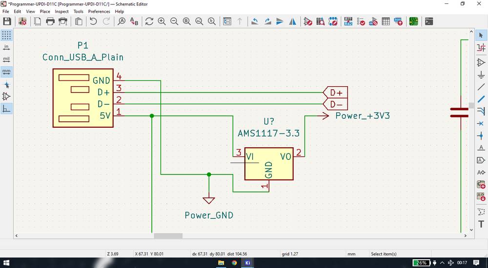
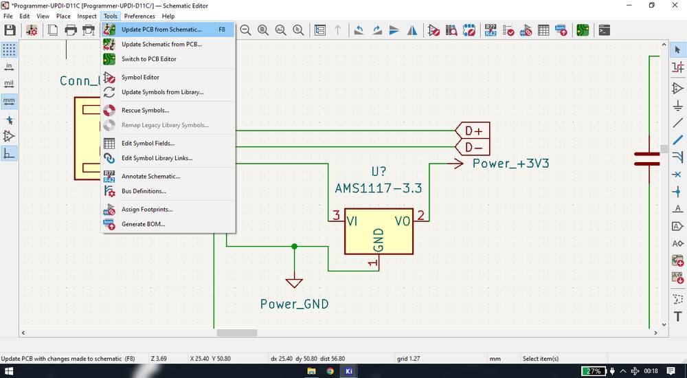
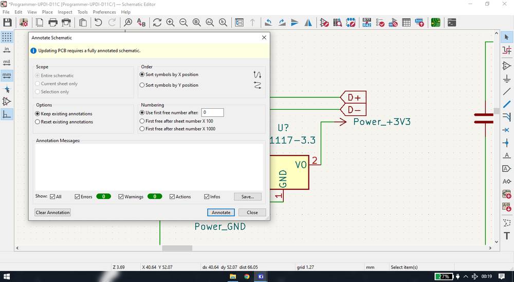
AFter that go to Tools and select Update PCB from schematic. If you are asked to annote the schematic, click on the annote button.
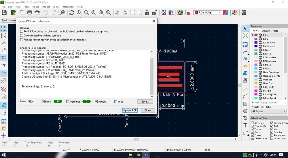
After that it will re-direct you to the board environment, there you'll be asked if you want to update the PCB, click on Update PCb,
(Earlier, what i used to do was replace and rewire the component in the schematic and then go to the PCB to see if there are any changes reflected,
because this is how you make changes in your PCB in eagle. Then i figured there was a refresh button in the Board environment but even after clicking
on that there was no change reflecting.)
After clicking on Update PCB, I finally saw the AMS1117 regulator showing in the board environment, however even after deleting the LM3480
regulator from schematc i was seeing that component in the board environment with the wires routed. So I first placed the AMS regulator somewhere
random and manually deleted the LM3480 regulator and placed the AMS1117 regulator in the place of LM2480 regulator and rerouted the wire.
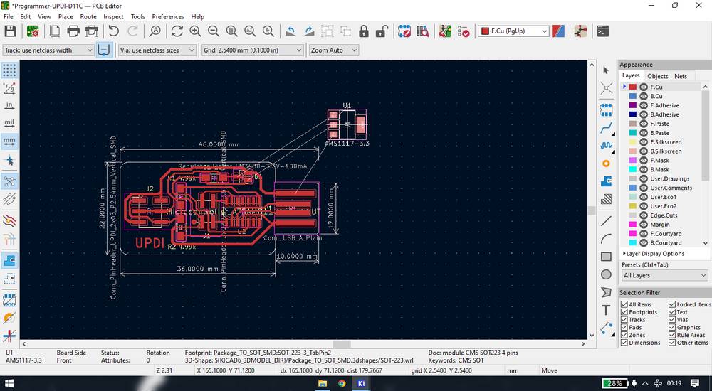
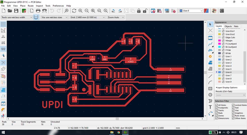
Since the AMS1117 package was larger than the LM3480, i had to make changes in the edge cut, and this was the final result.
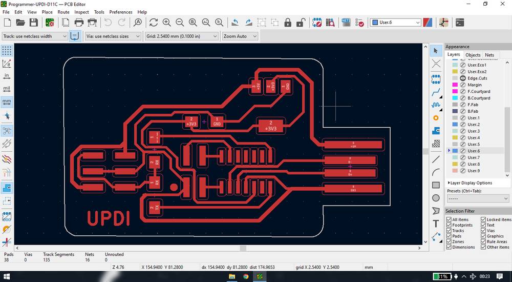
I then exported the inner and outer traces as black and white from KiCAD. The one thing i don't like about KiCAD is that it will export with
black color traces with white color background, so i had to invert the image from inkscape. The option of invert in mods doesn't work for me,
it just shows me a blank screen whe inverted.
((( consider putting image of this from mods)))
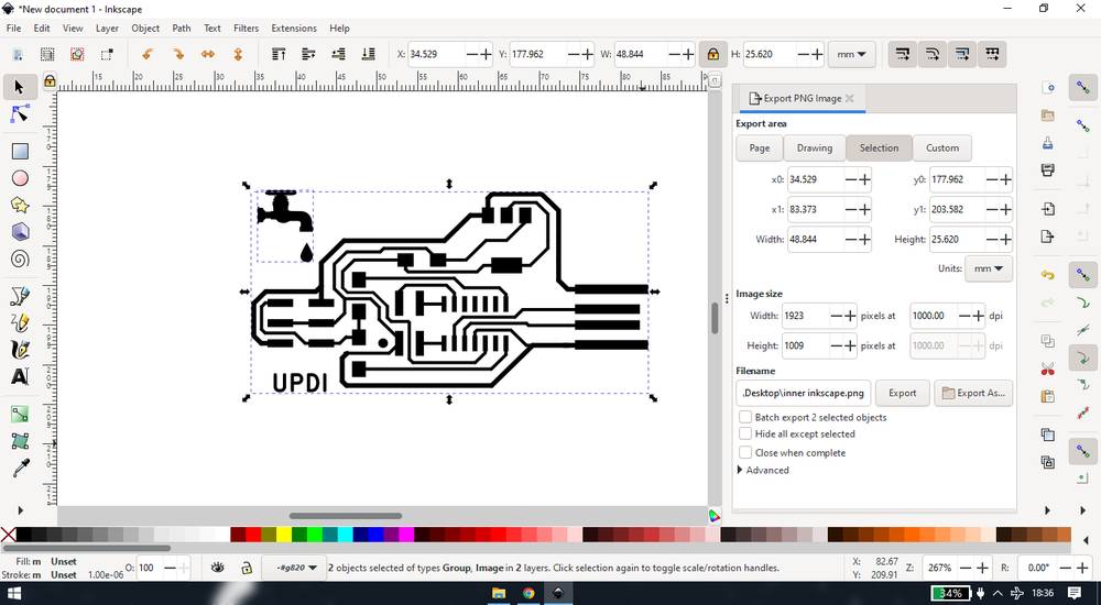
The exported file was in SVG format so i imported it to inkscape and added my final project logo(becase, why not).
This is the procedure i went through to export an inverted image,
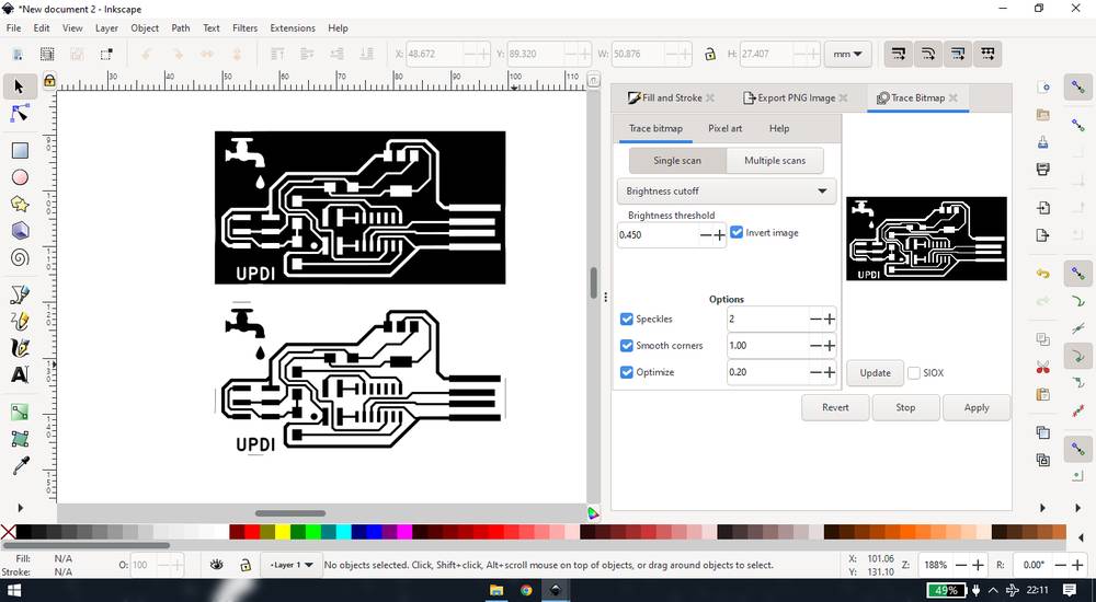
I imported the inner trace file and added the logo and exported the file in png format,
Create a new file and import the png file you just exported. Go to Path and select Trace Bitmap, with Brightness cutoff selected, check the invert
image option and click on apply. You will get the inverted image ready to generate the toolpath.
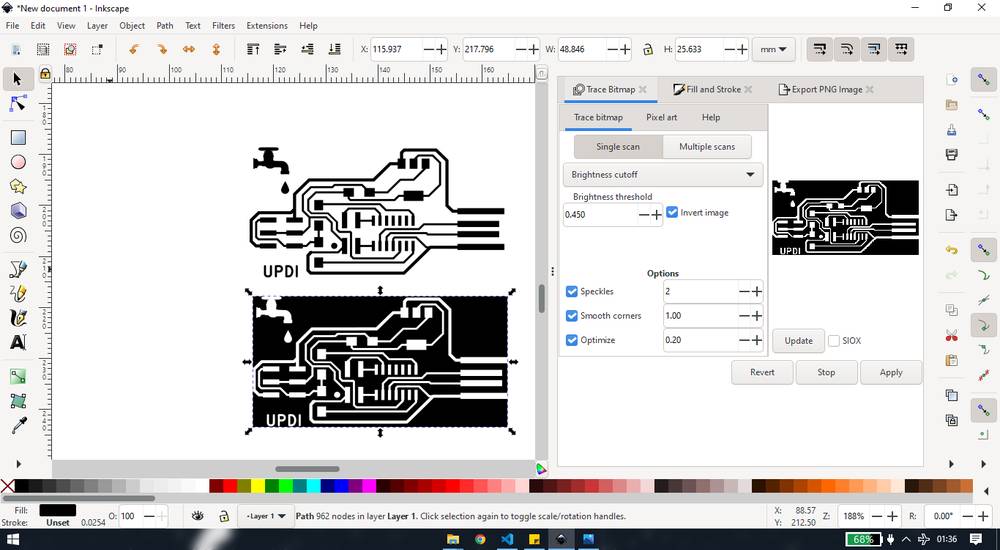
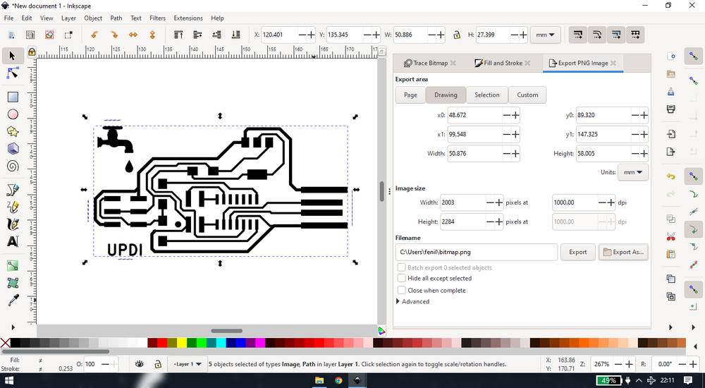
select the inverted image and export the image as png format with the help of selection tool. Do not forget to set the dpi to 1000 while
exporting.
This was the preview of the inner trace after i generated the toolpath,
The border of the inner trace was edge to edge due to which, few part of the trace won't cut properly so what i did was added a line on all
4 sides go make the border bigger than the trace.
this was the preview after generating the toolpath,
milling
I used the same broken vbit for doing the inner traces of UPDI.
This was the result of the trace with 0.0800mm cut depth and max depth,
just like before, the vbit didn't remove the copper properly so i retraced it with 0.0900mm cut depth and max depth and here is the result,
The traces were not proper and were full of burr. I then changed the vbit and traced the inner file with the same 0.0900mm cut depth and max
depth toolpath. And here are the results,
with the traces looking fine, i traced the outline file with 1/32 endmill,
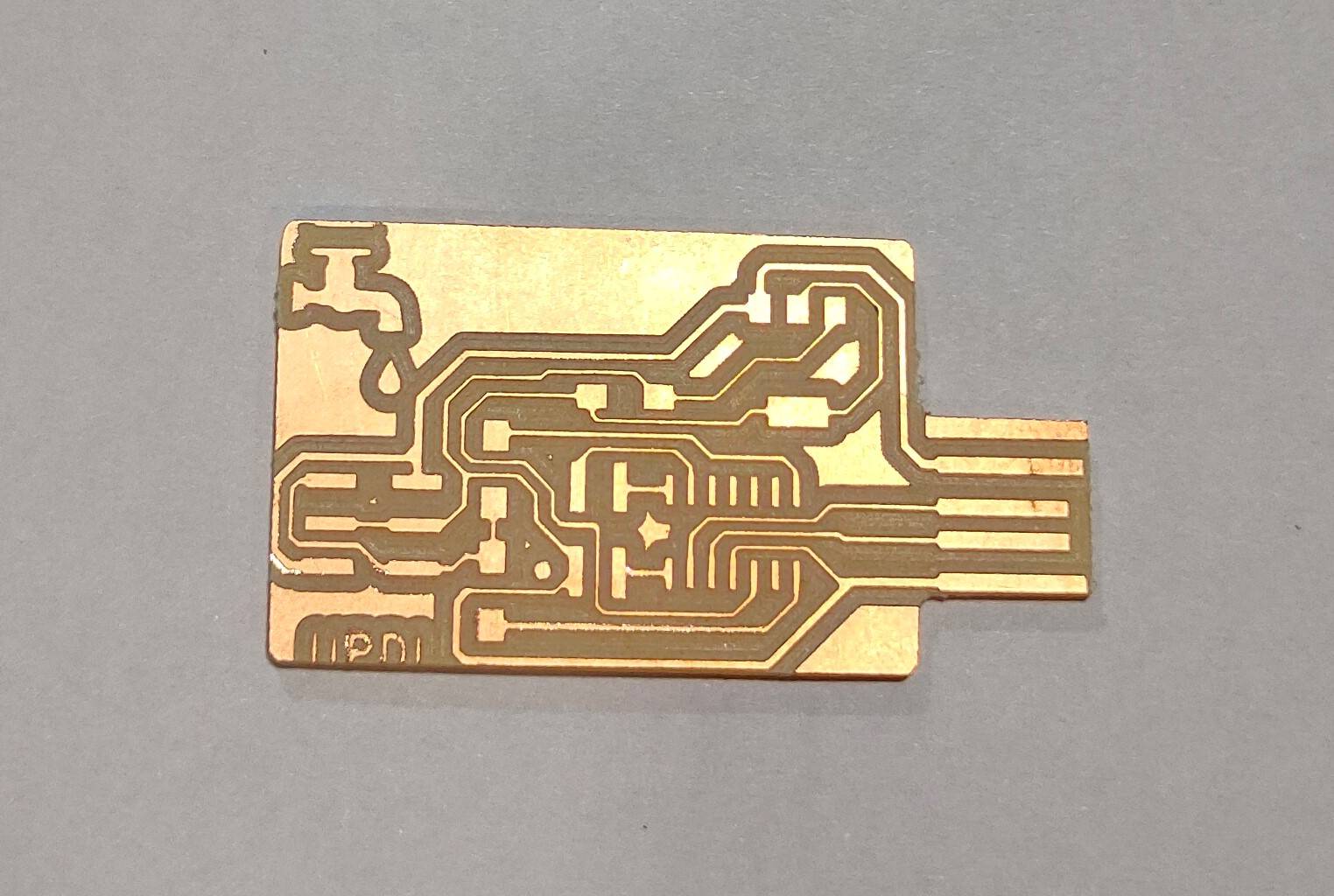
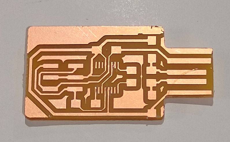
after little cleaning the PCB,
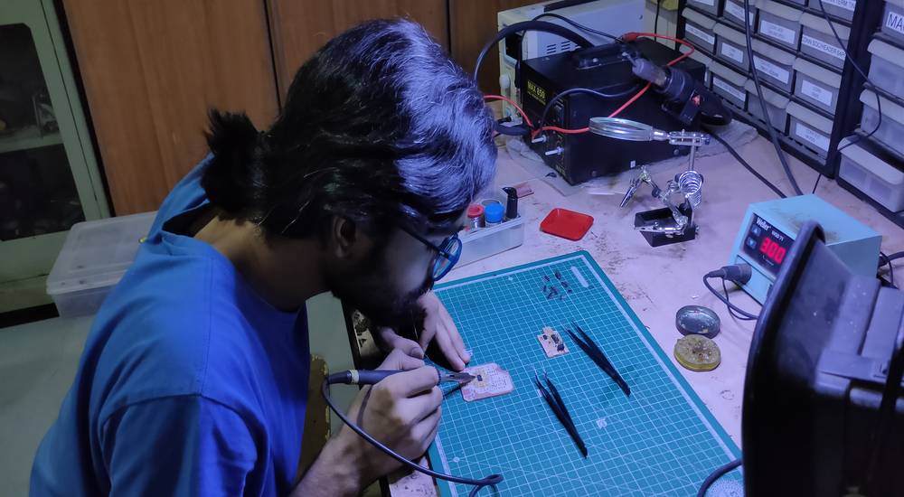
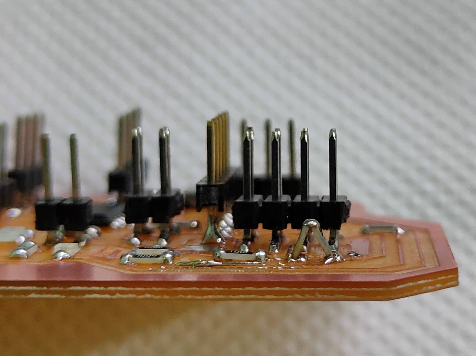
soldering attiny1614 and updi-samd11c board
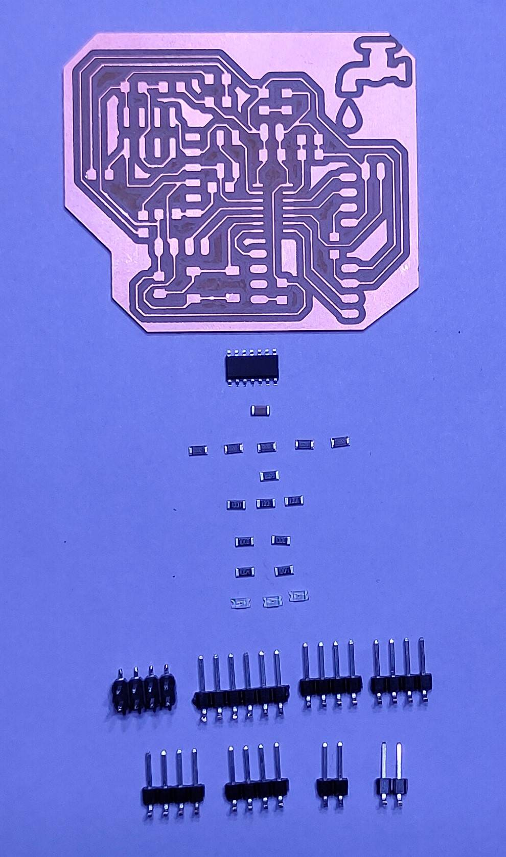
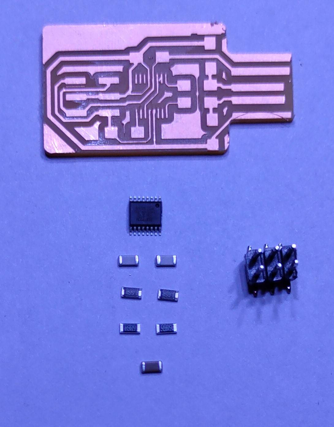
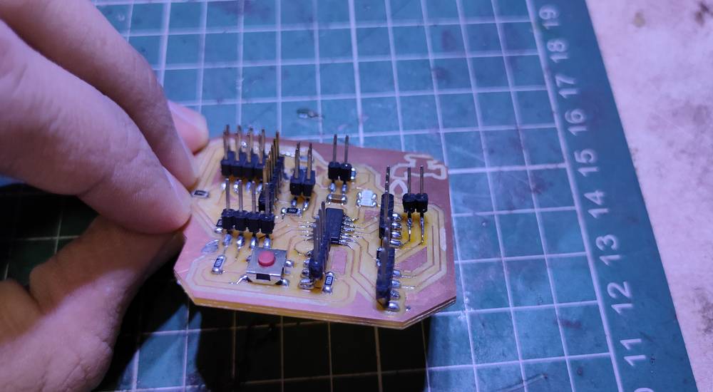
With the final project board and UPDI milled, i started gathering the componnets for soldering.
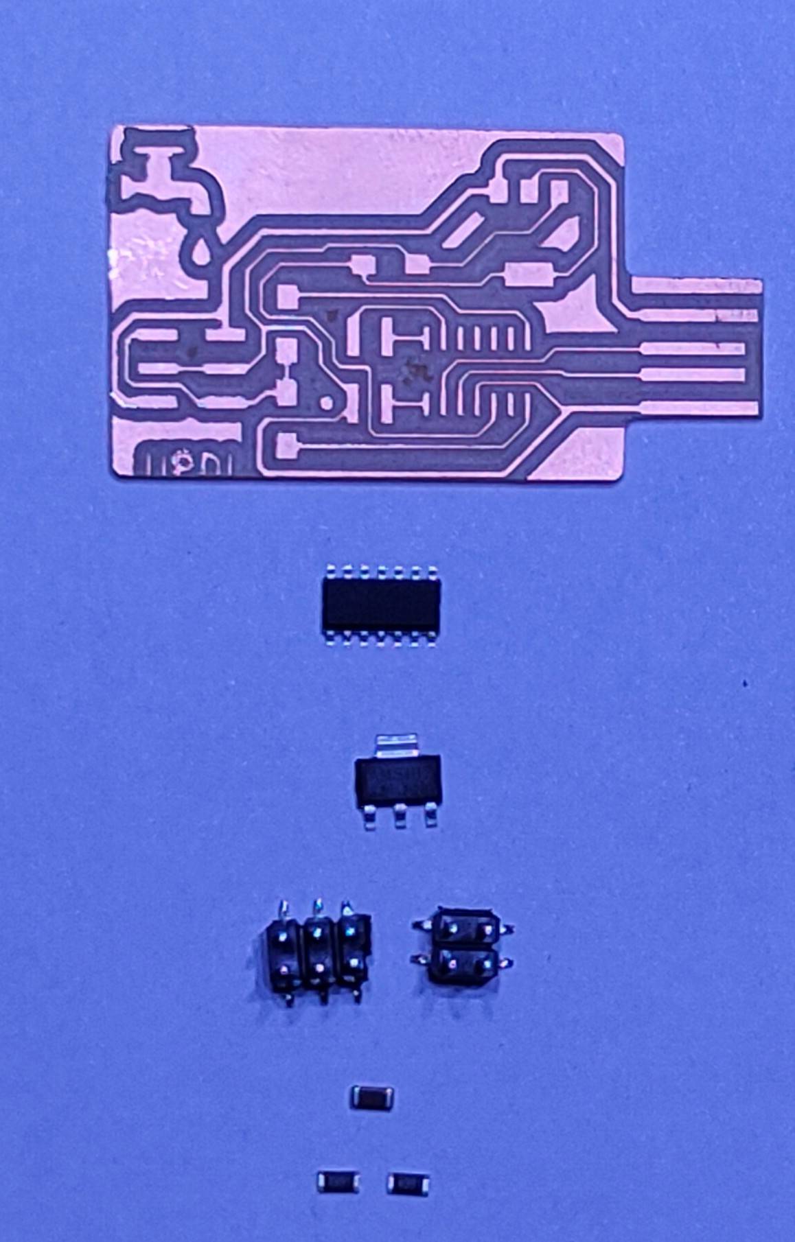
components used for updi are,
1x SAMD11C14 IC
1x AMS1117 3.3V regulator
1x 2x2 and 2x3 header pins (male)
1x 1uf capacitor
2x 4.99K ohms resistor
components used for final project board are,
1x attiny1614
1x 1uf capacitor
5x 0 ohms resistor
1x 49.9 ohms resistor
3x 1K resistor (if you have 2K ohms resistor in your inventory, consider 1K and 2K ohms resistor instead)
2x 100 ohms resisotr
2x 1M ohms resistor
3x LED
1x 2x4 header pin (male)
1x 1x6 header pin (male)
4x 1x4 header pin (male)
2x 1x2 header pin (male)
1x push botton
I started with soldering the UPDI,
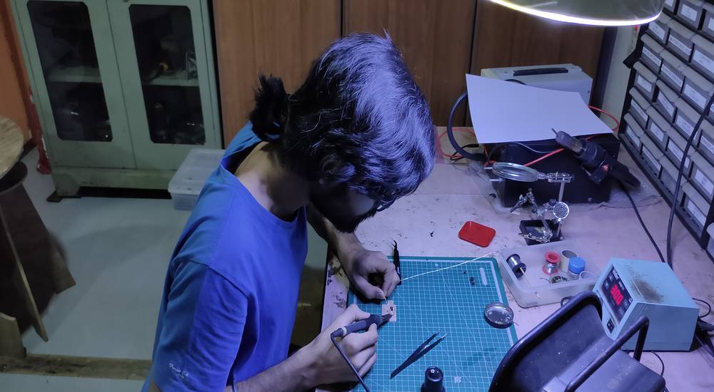
then i started soldering final project board,
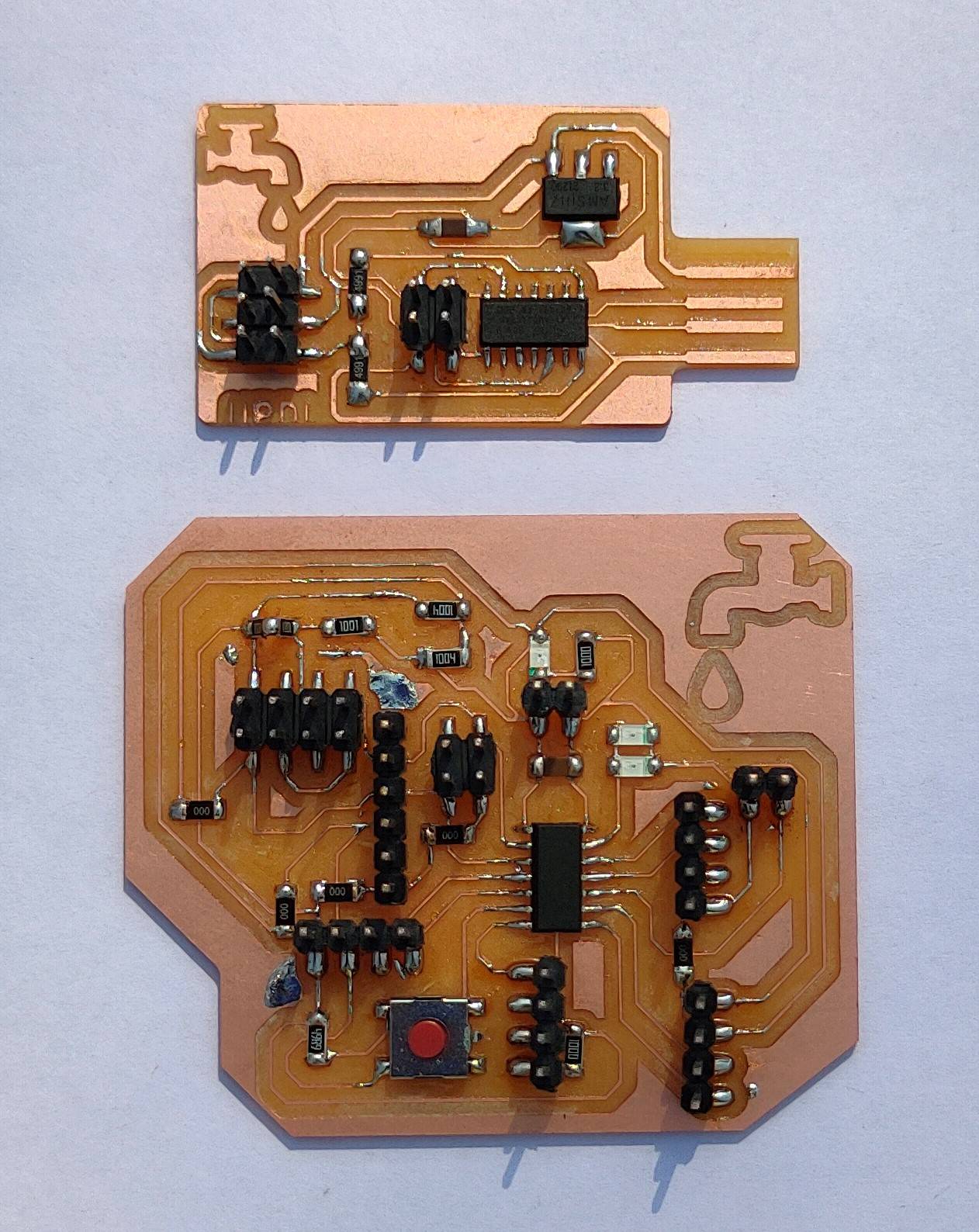
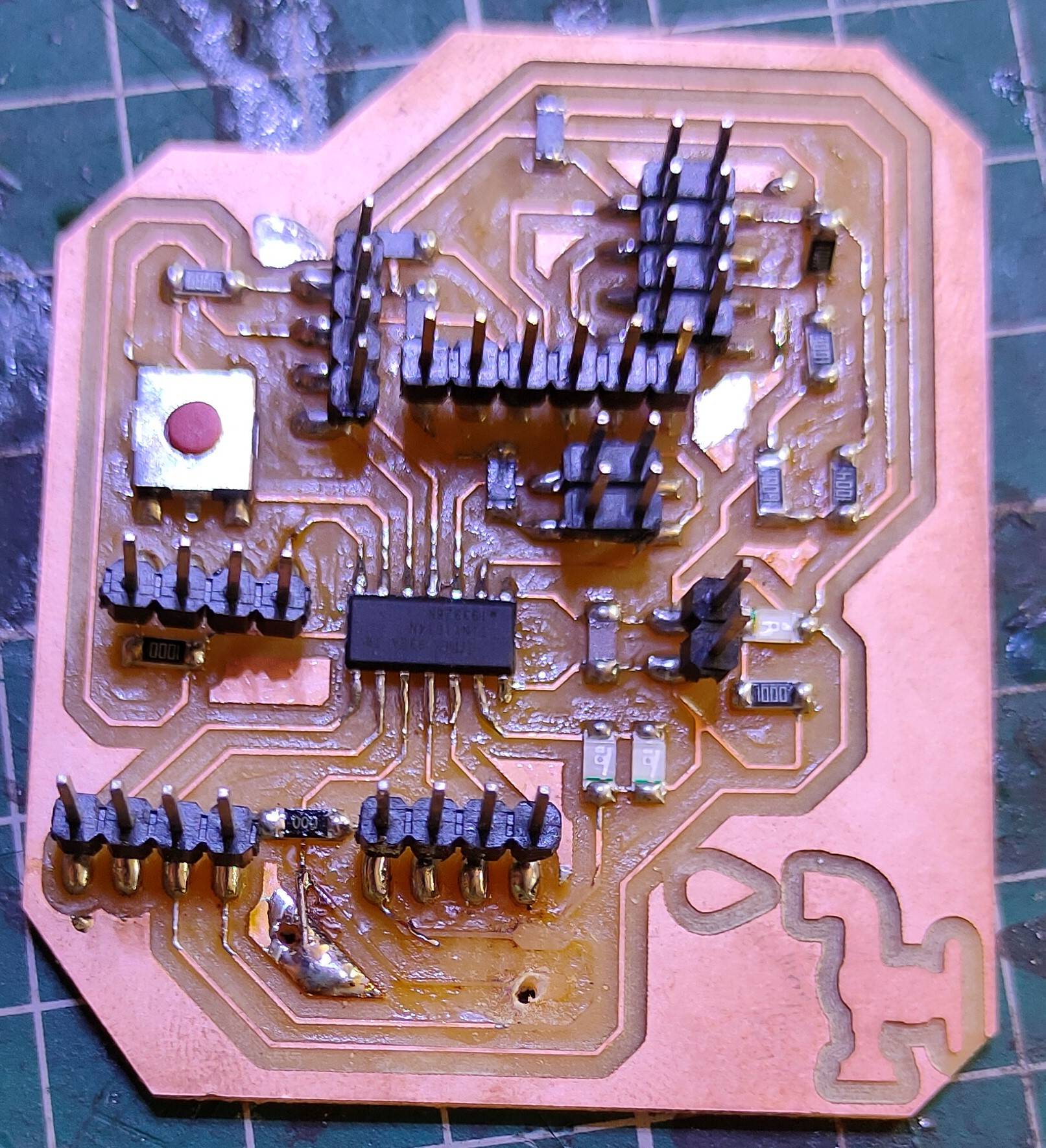
here are m final project board and UPDI stuffed,
While designing the final project board, i had given the provision for the voltage divider for converting 5V to 3V for the wifi module. The voltage
divider requires a 1K ohms resistor and 2K ohms resistor and i didn't checked the inventory so i didn't know we did not have a 2K resistor. So
i had to place 2x 1K ohms resistor in series but the board was already milled with only one pad for 2 resistor.
So this is how i placed 2 resistor in series on a single resistor pad,
Programming
For the programming part, me and my instructor started with refering to the Quentin's website:
http://fabacademy.org/2020/labs/ulb/students/quentin-bolsee/projects/samd11c_uart-updi/
.
We then downloaded the sam_ba bootloader and the zip file of the edbg(i was suppose to download the exe file).
I was using the MAX32625PICO board for programming the UPDI-d11c. I connected the Reset - Clock - Digital Input/output - Gronnd pin of the
MAX32625PICO to the UPDI by cutting the pin of through hole resistor and soldering it on one end of the jumper wire.
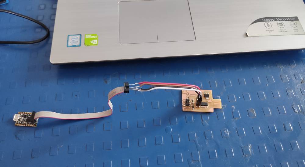
And then connected the MAXPICO board and UDPI to the PC,
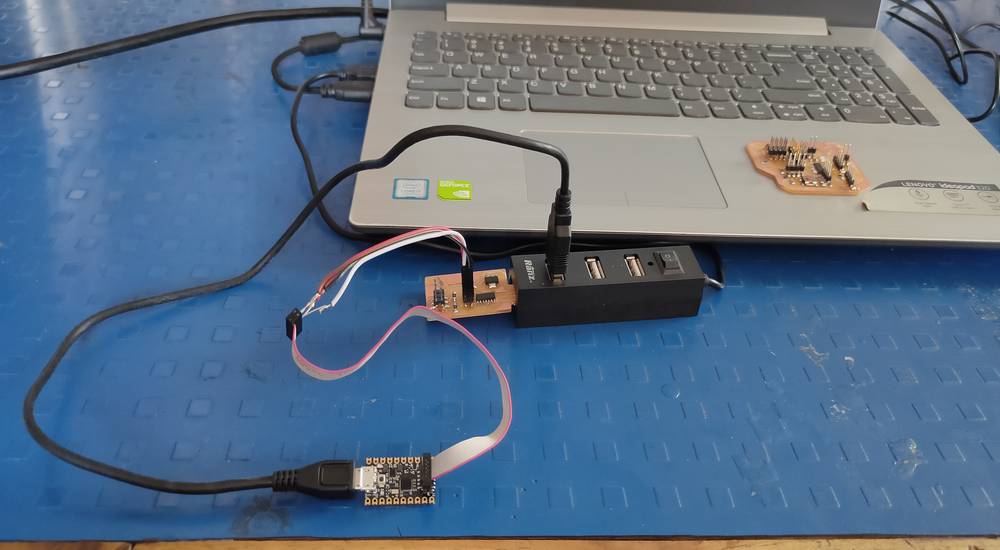
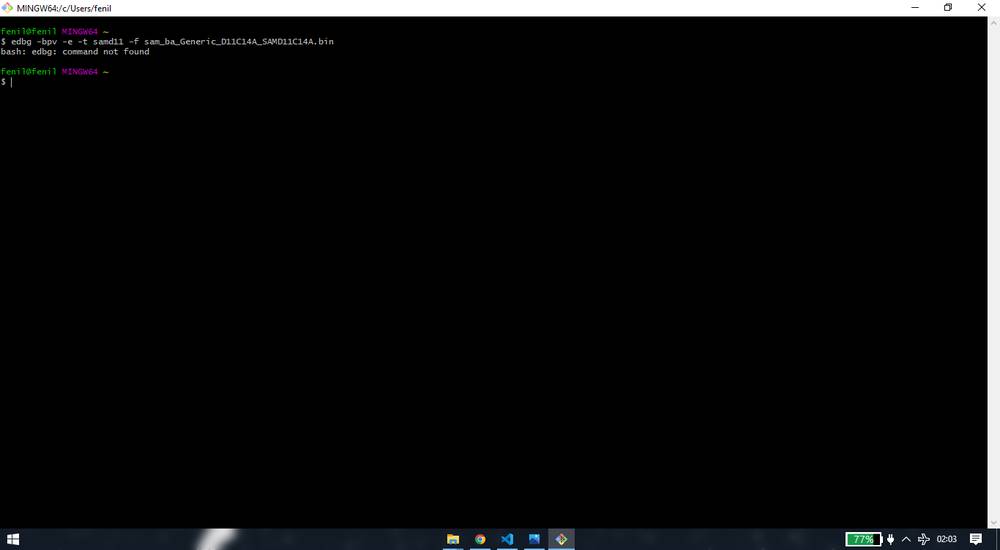
With the UPDI and MAXPICO board connected, we first ran this code,
edbg -bpv -e -t samd11 -f sam_ba_Generic_D11C14A_SAMD11C14A.bin
bu we were getting the error: bash: edbg: command not found .

We figured that we need to install the "edbg" . My instructor found this website from where i downloaded the edbg.exe file:
https://fabacademy.org/2021/labs/kannai/instruction/tips/fa2022_usbserial_win_edbg/
And later he found another website where we discovered that we need to give the file path of the edbg.exe file into the environment variables:
https://fab.cba.mit.edu/classes/863.21/Architecture/people/LauraMaria/index.html
So i followed the steps mentioned in that website:
Go to Setting > System > About > Advanced system settings > Environment Variables.
Inside environment variables select Path and click on edit. Click on new button and paste the file path where you have the edbg.exe file.
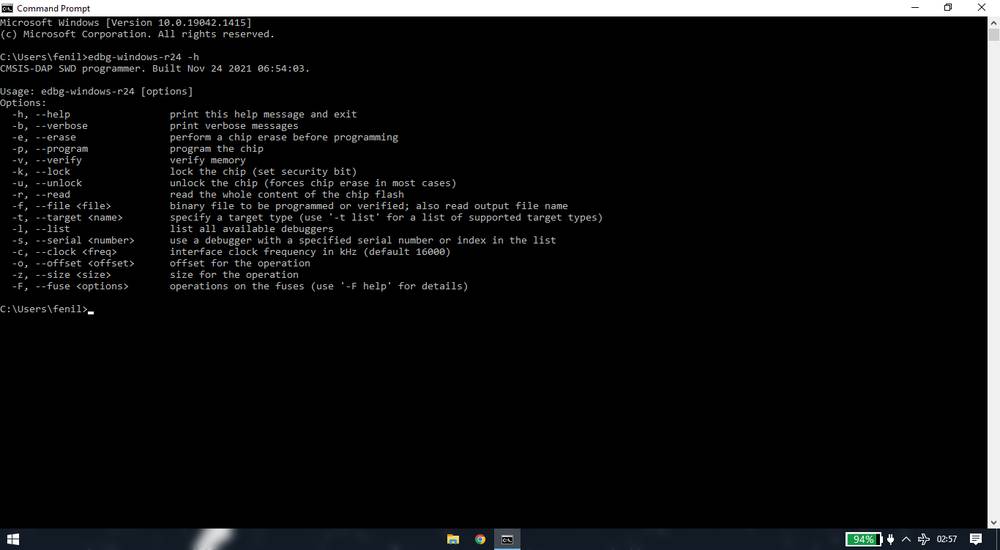
If i have given the file path correctly, if i run this code edbg-windows-r24 -h it should how you this results,
https://fab.cba.mit.edu/classes/863.21/Architecture/people/LauraMaria/assets/sucinstalledbg.png
Now what happened was that i had the edbg.exe file iny Downloads folder. When i copied the file path, it was only copying Downloads
instead of C:\Users\fenil\Downloads and when i pasted the path inside the environment variables it was showing juat
Downloads . So when i ran the edbg-windows-r24 -h command it was showing me this error,
I was arranging my files and shifted the edbg.exe file from Downloads to my Fab Academy folder in F drive and i thought let me try
it once again and this time code worked, becase i gave the correct file path.
I had the bootloader and the edbg.exe file in the same folder. So i open the gitbash by right clicking on the said folder and selecting Git Bash
here, this way i set the command directory to that particular folder. I then ran this command again with my UPDI and MAXPICO board connected
to the PC,
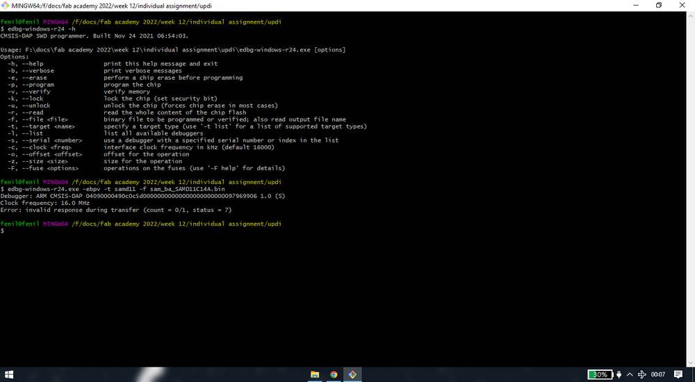
edbg -bpv -e -t samd11 -f sam_ba_Generic_D11C14A_SAMD11C14A.bin
and i was getting this error: "Error: invalid response during transfer (count = 0/1, status = 7)".
I tried checking the conection between PICO board and udpi but the connections were fine. I came accross a few websites where they had
mentioned the same error but not the solution. Then my instructor told me to make another UPDI with FT230XS IC where the IC wil be pre-programmed so i won't need to program
it.
updi - ft230xs
I downloaded the design files from here:
https://gitlab.fabcloud.org/pub/programmers/programmer-updi-ft230xs
Since the traces of the IC was very thin i had to use the 1/64 endmill because when i tried to mill with the broken VBIT, the traces were full
of burr.
I imported the SVG file of the inner tarce into mods and then inverted the image and then generated the toolpath with the default settings.
when i milled the inner trace, the traces of the IC were hardly sticking onto the board. It was comming off and i had to press the trace down and
carefully aligned thr trace of the IC. In doing that i already broke a part of the IC(broke one pin of ic in half). You can see that in the
trace at the bototm,
I then again milled the inner trace wiht the same toolpath and this was the result, the trace on top,
If you have observed, both of the IC had two bridges between two pins. I tried to remove the bridge manually with the cutter but ended up
damaging the other traces.
I then open the board file and export the
SVG file of the inner trace and the edge cut. THen import the inner and edge cut into inkscape and export them as png file with 1000 DPI.
Again import that PNG file and draw line on four sides to make the border bigger and then export them as PNG file. THen import the PNG file with
extended border and then invert the image with the help of trace bitmap and then export the inverted image as PNG file with 1000 DPI. All these
because i thought it might help me getting rid of the bridge.
I then again generated the toolpath with new files i made in inkscape and this is the preview of the trace,
I milled the inner traces wiht 1/64 endmill and this time there were 3 unnecessary bridges!(the one on top row is necessary)
I then took help of my colleague, Ashish Shende to remove the bridge and he too used the cutter to remove the bridge, but i guess he has more patience then me!
((( add photo of cutting the bridge )))
THis was the result after removing the bridge,
Once the board was ready i started gathering the components and started the soldering. These are the components i used,
SOldering the FT230XS IC was the hardest part given how thin the pins of IC are.
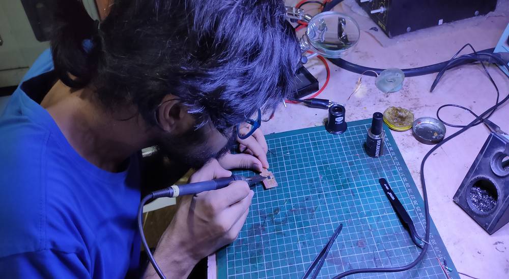
No matter how hard i tried, i was accidentally making solder bridges onto the IC. I had to use eye loupe and solder wick in order to remove
them,
((( image with eye loup yet to click)))
While removing bridges, i am sure i atleast removed one trace on the board but it has to be the trace of the pin on the IC which was not in use.
After a lot of patience my UPDI with FT230XS was ready,
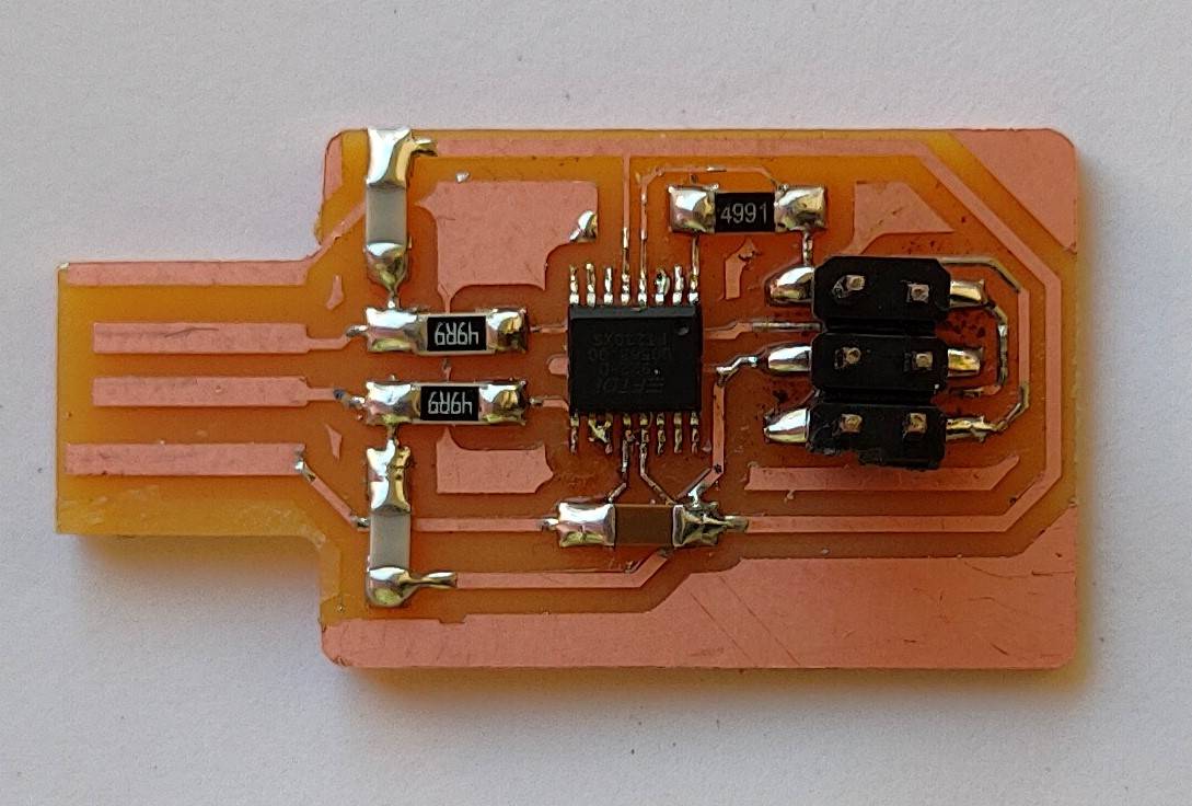
Now it was time to program to see if my final project board and the UPDI - FT230XS are working or not.
To upload the code i was using Arduino IDE. I installed a library called "megaTinyCore" by Spence Konde from tools > Board > Board Manager.
Make sure you have this link pasted in Additional Boards Manager URl's : http://drazzy.com/package_drazzy.com_index.json .
Go to File > preference and you'll find Additional Boards Manager URL.
After installing the library and seledcted these settings inside tools,

I uploaded the example sketch blink which you can find in File > Examples > Basics > Blink and here are the results,
I also designed and milled(with broken VBIT. The UPDI - FT230XS and the fabISP are the only two boards i milled with 1/64
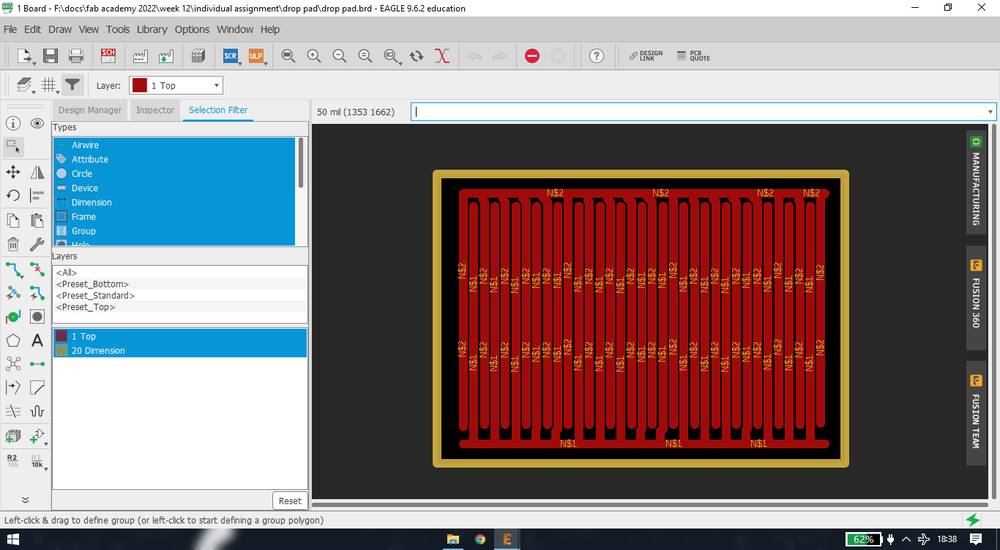
and rest all i have milled with broken VBIT) the rain drop like pad for detecting the drops,
Application
After the blink code was succesfully uploaded to the final project board with the UPDI-FT230XS it was concluded that the boards are working and
there is no issue with the connection or the soldering.
As mentioned above we had to add sensor to the microcontroller board and read the outcome so i tried ultrasonic sensor, step response and
rain drop sensor which was also the part of my final project,
Serial monitor
To read the data from any sensor with the help of Arduio board, you just need to upload the code with Serial.begin (9600); and
Serial.println(""); without adding any library and just open the serial monitor and you'll be able to read the data. However, to
ready the data from the board with attiny1614 chip, you need to install the library called SoftwareSerial: https://github.com/PaulStoffregen/SoftwareSerial
You can add the library from Arduino IDE by going to Sketch > Include library > add .ZIP library.
<<<---WIRING--->>>
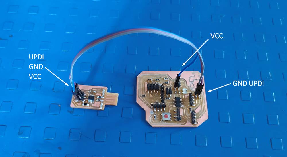
To avoid any confusion, i am naming UPDI-GND-VCC pins as UPDI pins and GND-CTS-VCC-TX-RX-RTS pins as Serial pins.
The programmer i made, UPDI-FT230XS, doesn't have the Serial pins, instead it has UPDI pins. So in order to read the data into the serial
monitor, my local instructor suggested to make the Serial UPDI converterter.
Generally, people have the Serial pins into their UPDI programmer
and then uses Serial UPDI converter to convert Serial pins to UPDI pins, in my case I was doing the reverse, converting the UPDI pins to Serial
pins with the help of Serial UPDI converter.
Here is the connection I was using to just uplaod the code into my final project board,
And here is the connection i use for reading the data into the serial monitor,
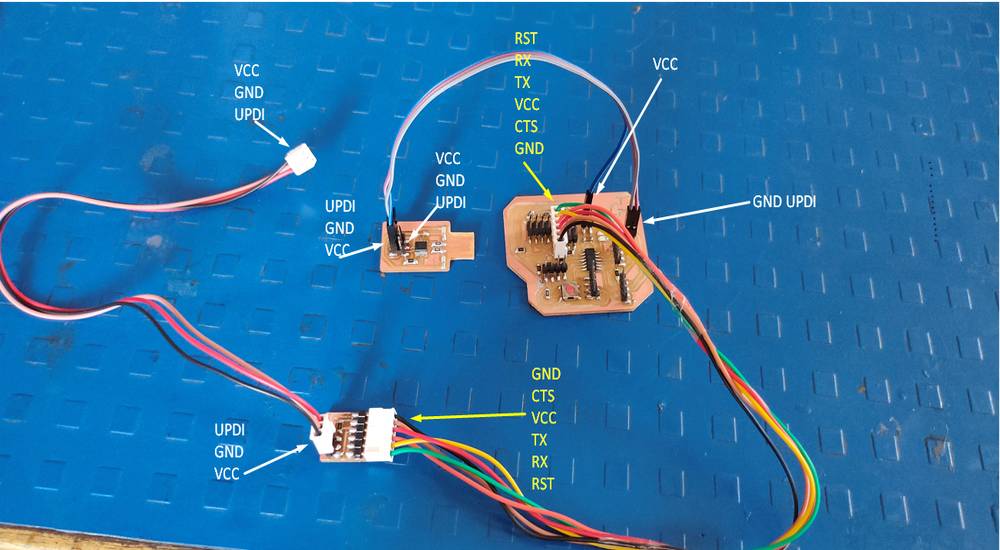
I was not able to uplaod the code if the RX-TX pins of the UPDI and final project board is connected so i used to dicsonnect the UPDI pins from
the UPDI progreammer while the code was being uplaoded and then connect again to read the data into the serial monitor.
<<<---CODE--->>>
This is the simple code I was using for displaying the text "hello world"
you can copy the code from here too.
I edited his code from the example code which you can find from File > Examples > SoftwareSerial > SoftwareSerialExample.
<<<---OUTCOME--->>>
This is the outcome of the code,
Ultrasonic Sensor
To detect the human presence i am going to use the ultrasonic sensor, sice it gives me the feedback in the form of distance. The ultrasonic
sensor i am using is hc-sr04 ultrasonic sensor.
<<<---WIRING--->>>
So the ultrasonic has four pins: ground, VCC, trigger and echo. You can use any digital pin for the trigger and echo, however i have seen people
generally using the PWM pin for the echo. Here is the connection i used for ultrasonic sensor,
ultrasonic sensor attiny 1614
GND GND
VCC VCC
TRIGGER PA1
ECHO PA2
<<<---CODE--->>>
This is the code i used,
you can copy the code from here too.
Reference of the code: https://github.com/futureshocked/ArduinoSbS2017/blob/master/_0510_-_Ultrasonic_Distance_Sensor/_0510_-_Ultrasonic_Distance_Sensor.ino
<<<---OUTCOME--->>>
This is the outcome of the code,
Soil moisture sensor/Rain drop sensor
For detectng the drops, i tried using yl-69 sensor which is same for detecting rain drops and soil moisture.
<<<---WIRING--->>>
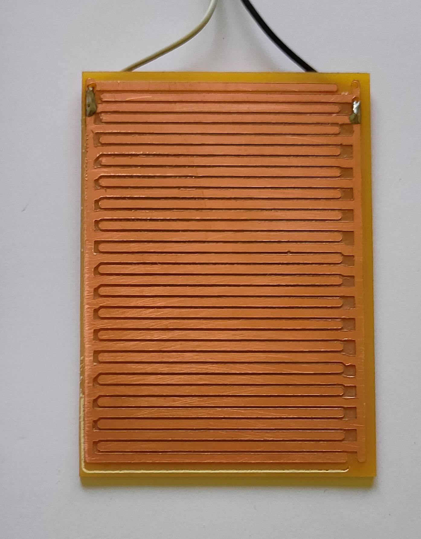
In the yl-69 sensor/module there are 6 pins. Four on one side and two on other side. The two pins are meant to be attached to the board with
comb like pattern made with two set of traces. I designed and milled a similar looking board,
the remainig four pins are ground-VCC-digital output pin-analog output pin. If you use the DO(digital output), the data you will get will be
in form of digital signal i.e. 0&1. If you use the AO(analog output pin) the data you'll get will be in form of analog signal i.e. 0 to 1023.
Here is the connection i used,
yl-69 attiny 1614
GND GND
VCC VCC
A0 PA6
<<<---CODE--->>>
This is the code i used,
you can copy the code from here too.
you can find this code from File > Examples > Basics > AnalogReadSerial.
<<<---OUTCOME--->>>
This is the outcome,
Step response
Since my final project board had the attiny1614 chip, instead of making separate module, i gave the provision of the step response onto my board
itself. Reference:
http://academy.cba.mit.edu/classes/input_devices/step/hello.txrx.t1624.png
http://academy.cba.mit.edu/classes/input_devices/step/hello.txrx.t1624.jpg
<<<---WIRING--->>>
Step response requires just 2 digital pins that act as TX-RX(transmitting and receiving). Now i had given the provision for TX-RX of wifi module,
step response and serial pins, all threee on same two pins i.e. RX-PA4 and TX-PA5 because i didn't had knowledge that I can define different
RX-TX pins for different modules and that RX-TX pins are nothiung but digital pins that transmit and receive signals. SO what was
happening was that the microcontroller can either show the data onto the serial monitor with
the help of RX-TX pins or it can collect the data from the step response with the help of same RX-TX pins, it cannot perform both of the task
at the same time, given that pins of both the module are connected on same pins. Until now i was only using the serial pins to read the data
into the serial monitor.
Since the step response just requires two pins as RX-TX and the the pins i had given provision for rain drop sensor had two pins too(pins can be
used as analog as well as digital) i connected the RX-TX pins of the pad into the pins that were assigned for rain drop sensor for the time being.
so i connected the TX pin to PA6 and RX pin to PA7.
<<<---CODE--->>>
This is the code i used,
you can copy the code from here too.
Source of the code: http://fabacademy.org/2020/labs/leon/students/adrian-torres/assignments/adrianino/step_response_txrx/step_response_txrx.ino
<<<---OUTCOME--->>>
This is the outcome,
Conclusion
Since the step responcse and the rain drop sensor was behaving in the same way for me, like for rain drop sensor the reading went from 1023 to
500 when the water was dropped on the pad and for the step response the reading went from 24K to 32K and since it would require me to
use a module for rain drop sensor while i just need to put two 1M ohms resistor for the step response, i decided to use te step response for my
final project. I have to re-design the board, i'll mention more on this in the final project tab.
If you have observed, two things were happening with the pad i was using for detecting water drops,
1- The water was sticking onto the pad and not sliding down easily,
2- I had to clean the pad/dehumidify the pad manually.
for the real application, i won't be cleaning the pad so what will happen is, a drop will get stuck on the pad and it will give false data of
the leakage until the drop evaporates. So dehumidifying the pad is going to be a challenge.
After testing the ultrasonic sensor, i accidentally pluck the two pins along with thre pads of my final project board, that were UPDI-GND,
I soldered the two pins onto mere trace lines and for better adhesion i used fevikwik gel,
The pins survived for a couple hours and then it came off again.
There was an unwanted pad near the trace of the UPDI pin so i bridged the trace and the pad with the pin of a through hole resistor and then
soldered a screw connector there,
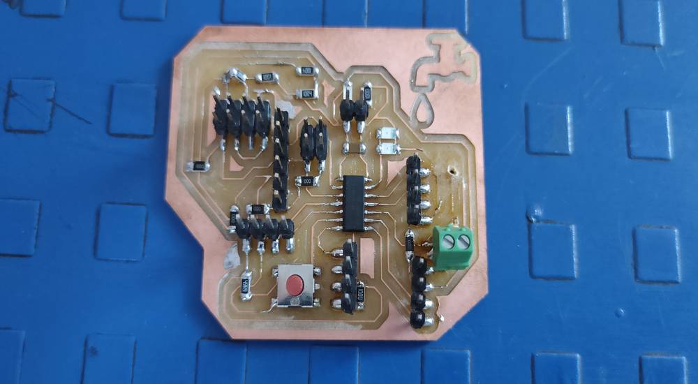
I didn't had single screw connector so i broke the pin of one connector and soldered only one pin of the screw connector(only one screw connector
is functional).
This week i learned how to select the IC of the board as per my requirements and how to define the pins as per the sensors i am using. I also
interfaced a few input devices with my attiny1614 board like ultrasonic sensor, YL-69 soil moisture module and step response. If you compare
the step response video of adrian:
http://fabacademy.org/2020/labs/leon/students/adrian-torres/images/adrianino/step1.mp4
and my step response video, you'll see a vast difference in the readings and the reason is the insulation between two electrodes and the number
of electrodes. Adrian was using just two copper plates while i was using multiple copper traces and so this is how it affected the readings.
Design files,
water drop pad
final project board
serial UPDI converter
UPDI-D11C
UPDI-FT230xs
Group assignment
For the group assignment we probed the analog and digital signals of IR sensor and Potentiometer. You'll find the details regarding the work done
in group assignment here:
https://fabacademy.org/2022/labs/vigyanashram/groupassig/groupassignment9.html
Drip Irritation by Fenil Chandarana is licensed under Attribution-NonCommercial-NoDerivatives 4.0 International![]()
![]()
![]()
![]()